
User's Manual


Page 24 Mainboard User's Manual
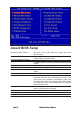
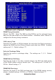
DRAM Timing Selectable
Manual / By SPD. Select "By SPD" to allow BIOS to get the optimized timing
data from the data stored on the DIMM modules. Otherwise, select "Manual" to
configure the following timing constraints.
CAS Latency Time
Specifies the number of SCLKs between the time when the Read command is
sampled by DRAM and the Whitney Sample reads data from DRAM. Available
settings are 2, 3. Default setting is "3".
Active to Precharge Delay
Specifies the active to precharge delay : The settings are 7, 6, 5. Default
setting is "7".
DRAM RAS-to-CAS Delay
Specifies the length of the delay inserted between the RAS and CAS signals
of the DRAM system memory access cycle. The settings are 2 SCLKs or 3
SCLKs. Default setting is "3".
DRAM RAS Precharge
Specifies the length of the RAS precharge part of the DRAM system memory
access. Available settings: 2 SCLKs, or 3 SCLKs. Default setting is "3".
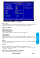
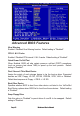
Advanced Chipset Features