
Data Sheet


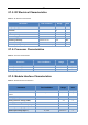
Table Of Contents
- 1. Production Introduction
- 2. Product Overview
- 3. Technical Specification
- Blank=Normal 85℃(Default)
- I=Industrial Application(Version for Hi-temp)
- 5. Contact Us

- 8 -
different environments.
At the same time, our company also provides a complete set of development and evaluation kits, users
can choose kits of different versions for testing and development according to their requirements.
3. Technical Specification
3.1. Electrical Specification
3.1.1. Electrical Specification
Table 3-1. Absolute Maximum Ratings
Parameter
Min
最Max
(VCC)Module input voltage(VCC)
1.85V
3.8V
Pin voltage (except ADC pin)
-0.3V
VDD_PADS+0.3
ADC Pin voltage
-0.3V
2.1V
Data of maximum drive current of all I/Os
50 mA
Maximum RF signal receiving density of chips
+10 dBm
Note: exceeding the absolute maximum ratings may damage module. In any case, the user shall not
violate the absolute maximum ratings listed in the previous table. If there is a violation, it may cause
irreparable damage to the module.
3.1.2. Test Conditions
Table 3-2. Test conditions(unless otherwise agreed), VCC = 3.3V, temperature = 25°C
Parameter
Range
Unit
Receiving current
12
mA
(@19dBm)Transmitting current
127
mA
Sleeping current
2.8
μA
Transmitting power
-9 to +19.5
dBm
Receiving sensitivity
-101
dBm