
Data Sheet
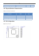
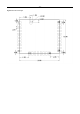


Table Of Contents
- 1. Production Introduction
- 2. Product Overview
- 3. Technical Specification
- Blank=Normal 85℃(Default)
- I=Industrial Application(Version for Hi-temp)
- 5. Contact Us

- 13 -
No. of
module
pins
No. of
QFN48
package
pins
Pin
signal
Direction
Pin specification
6
19
PD10
I/O
Digital I/O
7
20
PD11
I/O
Digital I/O
8
21
PD12
I/O
Digital I/O
9
22
PD13
I/O
Digital I/O; PTA_PRIORITY
10
23
PD14
I/O
Digital I/O; PTA_GRANT
11
24
PD15
I/O
Digital I/O ; PTA_REQUEST
12
27
PA2
I/O
Digital I/O
13
32
PB12
I/O
Digital I/O ;PTI_DATA
14
33
PB13
I/O
Digital I/O ;PTI_FRAME
15
12
nRESET
I
Active low chip reset (internal pull-up)
16
25
PA0
I/O
Digital I/O ;TXD
17
26
PA1
I/O
Digital I/O ;RXD
18
1
SWCLK
I/O
SWD Clock
19
2
SWDIO
I/O
SWD Data
20
35
PB14
I/O
Digital I/O ; VCOM_TX
21
36
PB15
I/O
Digital I/O ; VCOM_RX
22
43
PC6
I/O
Digital I/O
23
44
PC7
I/O
Digital I/O
24
45
PC8
I/O t
Digital I/O
25
46
PC9
I/O
Digital I/O
26
47
PC10
I/O
Digital I/O
27
48
PC11
I/O
Digital I/O
28
14,15,37
GND
-
Ground
29
9
,
18
,
34
,
40
3.3V
I
DC3.3V supply
30