
Specifications

Leader in IOT Embedded Solution
Page 8 of 15
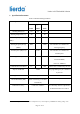
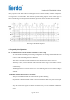
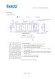
directly operated via the built-in MCU control register and the transceiver buffer, which can complete the
receiving function of wireless data. The read-write operation timing sequence of the module register is
shown in the drawing. For more operation information, please refer to the latest data manual CC2510.
Drawing 3-1 SPI Timing Sequence
4. Frequently Asked Questions
4.1 The communications cannot be made if the module is at close range
⚫ To verify whether the sending and receiving configurations are matching and the communications
cannot be made if the configurations are different.
⚫ The voltage is abnormal; and the transmission will be abnormal if the voltage is too low.
⚫ The battery is low; and the transmission will be abnormal if the voltage is lowered due to the low
volume battery.
⚫ The RF signal does not reach the antenna or π circuit soldering occurs error if antenna welding is
abnormal.
4.2 Module communication distance is not enough
⚫ The power transmitted is small due to bad antenna impedance matching.
⚫ Objects such as metal around the antenna or the metal inside the module may cause serious signal
attenuation.
⚫ Any other interference signals in the test environment may cause the module to communicate
close.