
Specifications

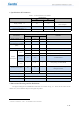
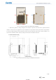
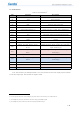
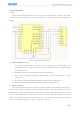
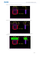
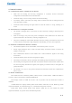
Table Of Contents

8 / 15
3 Basic Operations
3.1 Pins
When using the module, please choose the IO pin and carry out single-wire burning to the module
according to the actual application. It is suggested leaving VCC, GND and SWS on the bottom plate for
burning.
Fig. 3-1 Typical Application Circuits
3.2 Notices to Hardware Layout
1. Try to shorten the wire from the RF outlet to the antenna pad, lay the 50Ω impedance wire,
surround the wire with copper foil which is grounded, and form as many as possible through
holes around the wire.
2. If permitted, add the π circuit from the RF outlet to the antenna pad.
3. Make sure the surrounding environment of the antenna is clear, and at least leave a 5mm
clearance area.
4. Pay attention to the grounding quality, and large-area pavement is recommended.
5. Keep off the high-voltage circuits, high-frequency switches and other circuits.
3.3 Antenna Clearance
When using the PCB antenna of our company’s module, the following three schemes for the layout of
the RF clearance area are recommended. Usually, the RF performance of the module under Scheme 1 (The
PCB antenna is outside the board frame) is better than that of the module under Scheme 2 (The PCB
antenna is placed along the board side and its lower part is hollowed), and the RF performance of the
module under Scheme 2 is better than that under Scheme 3 (The PCB antenna is placed along the board
side and is not clad with copper), i.e. Scheme 1 ≥ Scheme 2 ≥ Scheme 3.