
Specifications

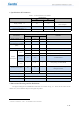
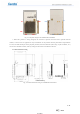
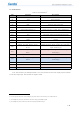
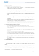
Table Of Contents

7 / 15
2.2 Pin Definitions
Table 2-1 Pin Definitions
2
PIN
Pin Name
Description
P1
GND
Ground
P2
ANT
RF signal/ANT
P3
GND
Ground
P4
RST
Power on reset ,active low
P5-P13
NC
P14
SWS/UART_RTS/PA<7>
Single wire slave / UART_RTS / GPIO PA[7]
P15
GND
Ground
P16
VCC
3.3V power supply for module internal circuit
P17
VCC
3.3V power supply for module internal circuit
P18
GND
Ground
P19
SWS/UART_RTS/PA<7>
Single wire slave / UART_RTS / GPIO PA[7]
P20
PWM3_N/UART_RX/sar_aio<9>/
PC<5>
PWM3 inverting output / UART_RX / SAR ADC
input / GPIO PC[5]
P21
PWM4
3
/UART_TX/sar_aio<1>/
PB<1>
PWM4 output / UART_TX / SAR ADC input /
GPIO PB[1]
P22
The same as P21
The same as P21
P23
PWM3
4
/UART_RX/sar_aio<0>/
PB<0>
PWM3 output / UART_RX / SAR ADC input /
GPIO PB[0]
P24
GND
Ground
P25
The same as P21
The same as P21
P26
The same as P23
The same as P23
Note: This module is pin-multiplexed.that is, P21, P22, and P25 are the same output port,P23 and P26
are the same output port. This module can output 2 PWM.
2
For the specific functions of the multiplex pin, please refer to the Datasheet for TLSR8250F512
3 pin-multiplexed, P21, P22, and P25 are the same output port,PWM4 output
4 pin-multiplexed, P23, and P26 are the same output port,PWM3 output