
Specifications

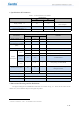
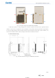
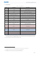
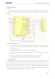
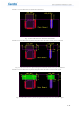
Table Of Contents

5 / 15
1 Specifications & Parameters
Table 1-1 Limit Parameters of Module
Table 1-2 Working Parameters
1
of Module
Parameters
Performance
Remarks
Min
TYP
Max
Supply voltage(V)
2.7
3.3
3.6
Work temperature(℃)
-40
-
85
Initial frequency tolerance
(KHz)
-30
-
+30
Below 25℃
Work frequency (GHZ)
2.402
-
2.480
Support customized frequency setting
Power
consumption
Transmit
(mA)
17
18
20
Output power 10dBm,system timer 16MHz
5.5
6.8
8
Output power 0dBm,system timer 16MHz
Receive
(mA)
5.5
6.5
7.5
Overall current
Sleep
(uA)
-
0.15
1
Deep sleep, n
ot save SRAM
Transmit power (dBm)
-25
10
-
Transmit power can be configured
through software
RSSI (dBm)
-95
-96
-
1Mbps,PER<30.8%
Communication protocol
BLE5/4.2/Mesh
Interface type
stamp /side inserted
Dimensional accuracy
GB/T1804-C level
Meet the dimensional tolerance class C
2 Dimensional Drawing and Pin Definitions
The physical diagram of LSD4BT-K53ASTD001 is as shown in Fig. 2-1. There will be a label on the
shield cover, and it shall be subject to the physical product.
1
The test is conducted at 25℃ in a shielded room environment.
Parameters
Performance
Remarks
Min
Max
Supply voltage (V)
-0.3
+3.6
All AVDD and DVDD with
same voltages
Max voltage of input pins
-0.3
VDD+0.3
Storage temperature(℃)
-65
150