User Manual Product Name: E92 BLE Module Product Model: LSD4BT-E92ASTD001 Version: Rev01 1
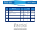
Revision History Serial No.
Contents CHAPTER 1 OVERVIEW.........................................................................................................................4 1.1 FUNCTIONAL CHARACTERISTICS........................................................................................................ 4 1.2 APPLICATION OCCASIONS................................................................................................................... 5 CHAPTER 2 SPECIFICATION & PARAMETERS..............................................
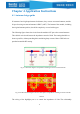
Chapter 1 Overview E92 series of Bluetooth module is high-performance Bluetooth module which is based on the low power consumption NORDIC Bluetooth SOC chip nRF52 series (support BLE 5.0) . The module adopts stamp hole-type interface, and with two antenna options : PCB antenna and external antenna, which is compatible with E66 series module . The key features of the module is low-power consumption, small size and high anti-interference ability.
● programmable peripheral interface (PPI) ● DC-DC working mode ● Support user defined download protocol ● 3 SPIs ● 2 TWIs ● 1 UART ● 3 PWMs ● 8 10/12bit ADCs 1.2 Application Occasions ● 2.
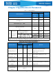
Chapter 2 Specification & Parameters Table 2-1 Limit Parameters Performance Main Parameters Maximum Value Value Power supply voltage(V) -0.3 3.9 IO voltage(V) -0.3 VDD+0.
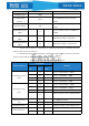
Number of channels 40 Modulation type GFSK Communication distance1 Connection distance2 Transmittance power (dBm) Receiving sensitivity (dBm) Receiving sensitivity (dBm) 1. @3.3V;4dBm;BLE mode-1M ;PCB 100m antenna @3.3V;4dBm;BLE mode-1M ;PCB 50m antenna @3.
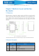
1. CPU clock speed is 64MHz, set external as idle status, supply voltage is 3.3V Chapter 3 Hardware Layout and Interface Description 3.1 Dimensions When this product is designed, the tantalum capacitors and PCBs have optional material models. On the premise that the performance requirements are met, the appearance color may be different, and the actual product shall prevail. The main materials (main chips, crystal oscillators, etc.) do not have any substitutional models.
5 P0.30/AIN6 Digital I/O pin; analog I/O pin 6 P0.31/AIN7 Digital I/O pin; analog I/O pin 7 P0.02/AIN0 Digital I/O pin; analog I/O pin 8 P0.03/AIN1 Digital I/O pin; analog I/O pin 9 P0.04/AIN2 Digital I/O pin; analog I/O pin 10 VBAT Power supply 11 GND PWR GND 12 RSTN RESET 13 SWDCLK Clock debugging pin 14 SWDIO Data debugging pin 15 P0.07 Digital I/O pin 16 P0.08 Digital I/O pin 17 P0.14/UART_TX Digital I/O pin; serial data TXD pin 18 P0.
Chapter 4 Application Instructions 4.1 Antenna design guide If customers have high requirements for distance, they can use an external antenna, and the IO port for using an external antenna is PIN27 (ANT). The bottom of the module, including the original antenna position, should be completely covered with copper. The following figure shows the circuit from the module ANT pin to the external antenna. The red thick wire should ensure the impedance control of 50Ω.
between plate thickness, line width and line spacing can be referred as following: FR4 double-sided boards recommended value (H=Board thickness,W=Line width,D=Spacing between wiring and copper-clad) H=1.0mm,W=0.8mm,D=0.2mm H=1.0mm,W=1.0mm,D=0.254mm(Recommended) H=1.2mm,W=1.0mm,D=0.2mm(Recommended) H=1.6mm,W=1.0mm,D=0.2mm (Recommended) (Ask Lierda engineer for more design support) 4.2 Notice for base board layout Save enough clearance zone for antenna .
4.3 Notices 1. Power Supply It is suggested supplying power to the module with DC regulated power supply. The ripple of power supply should as small as possible. Usually the ripple is less than 30 mV. Excessive ripple will lead to poor sensitivity and other connection abnormalities.
the land after more than 3 months, and may lead to such problems as false welding and missing welding during the mounting process. In order to ensure the pass rate of reflow, it is suggested picking 10% of products for visual inspection and AOI detection in the first time of mounting, so as to ensure the reasonableness of the furnace temperature, device absorption method and placement method; Operators at all stations must wear the anti-electrostatic gloves during the whole production process; 5.
Chapter 6 Product Package 6.1 Packaging Method Tape Foam Electrostatic bag 6.2 Strip Size 6.3 Product Direction The placement direction of the tape packaging module is shown as following: Protecting tape Cover tape Round hole Depression Carrier tape rubber wheel Product information label Carrier tape Discharge direction Notice To users Welcome to use the products of Lierda Science & Technology Group Co., Ltd..
Regulatory Conformance (RED) Hereby, Zhejiang Lierda Internet of Things Technology Co.,Ltd declares that the radio equipment type LSD4BT-E9x is in compliance with Directive 2014/53/EU. The full text of the EU declaration of conformity is available at the following website:https://www.lierda.com/ Radio specification Frequency Range Max.RF power 2402-2480MHz 7.
- Reorient or relocate the receiving antenna. - Increase the separation between the equipment and receiver. -Connect the equipment into an outlet on a circuit different from that to which the receiver is connected. -Consult the dealer or an experienced radio/TV technician for help - This device and its antenna(s) must not be co-located or operating in conjunction with any other antenna or transmitter.
Instructions to the OEM/Integrator: This module has been granted modular approval for mobile applications. OEM integrators for host products may use the module in their final products without additional FCC certification if they meet the following conditions. Otherwise, Additional FCC approvals must be obtained. The OEM must comply with the FCC labeling requirements.