
User Manual

Control Technique
3-Phase BLDC Motor Control with Sensorless Back-EMF, ADC, Zero Crossing, Rev. 3
18 Freescale Semiconductor
Preliminary
As stated, the AD converter has individual ADC Offset Registers for each ADC channels. The value in the
Offset Register can be subtracted from the AD conversion output. The final result of the AD conversion is then
two’s compliment data. The other feature associated to the Offset Registers is the Zero Crossing interrupt. The
Zero Crossing interrupt is asserted whenever the ADC conversion result changes the sign compared to the
previous conversion result. Refer to the manual for detailed information.
This application utilizes ADC Zero Crossing Interrupt to get the Back-EMF Zero Crossing event.
5.3.1.2 ADC Zero Crossing Offset Setting
As explained in the previous section, the ADC Offset Register is set to one half of the DC-Bus value. This is
valid at the following conditions:
• Motor phases are symmetrical (all 3-phases have same parameters)
• hardware dividers for the ADC of the DC-Bus and all 3-phase voltages, have equal ratio
The ADC Offset Register needs to be continuously updated, to reflect the DC-Bus voltage variation caused by
the ripple of DC-Bus voltage.
The above mentioned conditions are not 100% fulfilled in real drive due to the unbalance in real sensing
circuitry and the motor phases. Therefore, the real application must compensate such unbalance.
The presented application first sets the ADC Offset Registers[0..3] of all 3-phases to:
• ADC Offset Register[0..3] = Calibration Phase Voltage Coefficient * DC-Bus
Where the Calibration Phase Voltage Coefficient is set to 0.5. Later during the Alignment state the Calibration
Phase Voltage Coefficient is further corrected. The DC-Bus and non-fed phase branch voltage are measured
and the correction is calculated according to the following formula:
Calibration Phase Voltage Coefficient = (ADC Offset Register + Free Phase Branch Voltage)/DC-Bus voltage
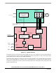
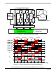
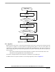
5.3.2 Back-EMF Zero Crossing Synchronization with PWM
The power stage PWM switching causes high voltage spike on the phase voltages. This voltage spike is passed
to the non-fed phase due to mutual capacitor coupling between the motor windings (see
Figure 5-4). Non-fed
phase “branch” voltage U
va
is then disturbed by PWM switching shown on phase branch voltage U
vb
.
u
va
u
vb
Zero Crossing Sample
s/w flag
Figure 5-4. Back-EMF Zero Crossing Synchronization with PWM