
User's Manual

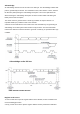


in the frame that follows
• The first byte of a frame indicates the device address according to the I2C-bus rules
• The second byte indicates the register address. No data bytes are added
• The Read/Write bit is 0
After the write access, read access can start. The host sends the device address of the
PN512. In response, the Module sends the content of the read access register. In one
frame all data bytes can be read from the same register address. This enables fast FIFO
buffer access or register polling.
The Read/Write (R/W) bit is set to logic 1.
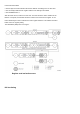
Register read and write access
I2C-bus timing