
Specifications


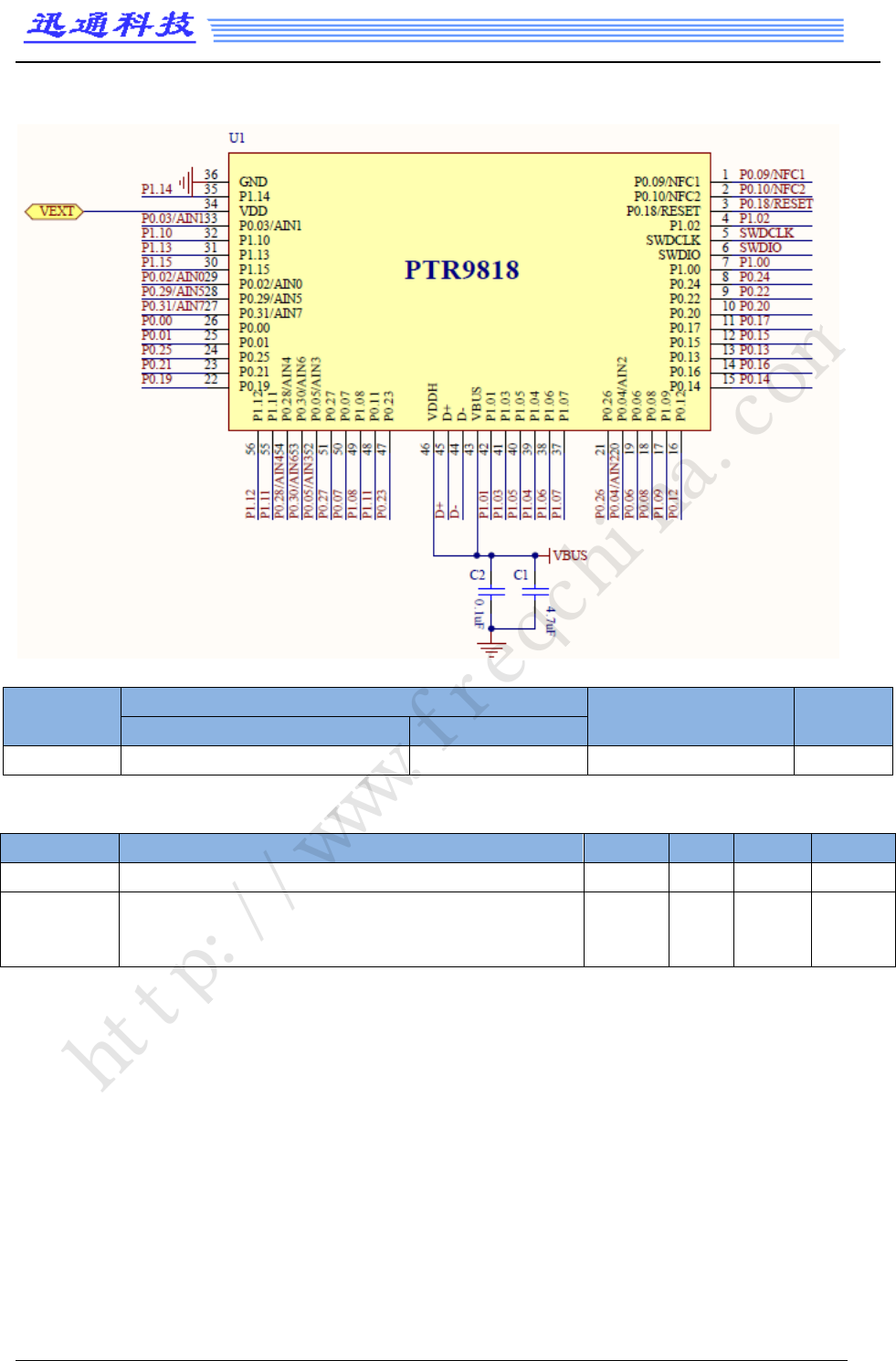
Reference Circuit configuration 5
Configurations summary for reference circuit 5
Config no.
Main Supply
EXT Supply Output USB
VDDH VDD
Config.5 USB(VDDH = VBUS) N/A Yes Yes
Explanation of symbols in reference circuit 5 schematic
Symbol Parameter Min. Typ. Max. Units
V
BUS
Supply voltage on VBUS pin 4.35 5 5.5 V
V
EXT
Voltage output on VDD when supplied from internal
regulator (REG0). V
BUS
is the input to REG0.
1.8 3.3 V
Some general guidance is summarized here:
Main supply voltage is connected to VDD/VDDH. The system will enter one of two supply voltage
modes, normal or high voltage mode, depending on how the supply voltage is connected to these
pins. Normal voltage mode is entered when the supply voltage is connected to both the VDD and
VDDH pins (so that VDD equals VDDH).High voltage mode is entered when the supply voltage is
only connected to the VDDH pin and the VDD pin is not connected to any voltage supply.
By default, the LDO regulators in the chip are enabled and the DC/DC regulators are disabled.
Registers DC/DCEN0 and DC/DCEN are used to independently enable the DC/DC regulators.
External LC filters has been connected in the Module for DC/DC regulators being used.
The GPIO high reference voltage always equals the level on the VDD pin. In normal voltage
mode, the GPIO high level equals the voltage supplied to the VDD pin, and in high voltage mode
it equals the level specified in the register REGOUT0 UICR registers.
COPYRIGHT ©2018 ALL RIGHTS RESERVED XUNTONG Tech E-mail: nrf@freqchina.com
9
http://www.freqchina.com