
User's Manual
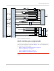
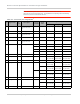
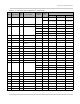
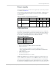
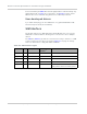
Table Of Contents
- Important Notice
- Safety and Hazards
- Limitation of Liability
- Patents
- Copyright
- Trademarks
- Contact Information
- Revision History
- 1: Introduction
- 2: Technology Overview
- 3: Standards Compliance
- 4: Electrical Specifications
- 5: RF Specifications
- 6: Power
- 7: Software Interface
- 8: Mechanical and Environmental Specifications
- 9: Regulatory and Industry Approvals
- A: Antenna Specification
- B: Design Checklist
- C: Testing
- D: Packaging
- E: References
- F: Acronyms
- Index

Product Technical Specification & Customer Design Guidelines
28 Proprietary and Confidential - Contents subject to change 2400074
37 GND V Ground Input Power - 0 -
38 USB_D+ - USB data positive Input/Output Differential - - -
39 VCC V 3.3 V supply Input Power 3.0 3.3 3.6
40 GND V Ground Input Power - 0 -
41 VCC V 3.3 V supply Input Power 3.0 3.3 3.6
42 WLAN_LED_N - LED Driver Output Low 0 - 0.45
43 GND V Ground Input Power - 0 -
44 GPIO4 - General purpose I/O Input high - 1.17 1.80 2.10
Input low - -0.3 - 0.63
Output high - 1.35 - 1.80
Output low - 0 - 0.45
45 NC - No connect - - - - -
46 GPIO5 - General purpose I/O Input high - 1.17 1.80 2.10
Input low - -0.3 - 0.63
Output high - 1.35 - 1.80
Output low - 0 - 0.45
47 NC - No connect - - - - -
48 GPIO6 - General purpose I/O Input high - 1.17 1.80 2.10
Input low - -0.3 - 0.63
Output high - 1.35 - 1.80
Output low - 0 - 0.45
49 NC - No connect - - - - -
50 GND V Ground Input Power - 0 -
51 NC - No connect
Reserved for future
use
- - - - -
52 VCC V 3.3 V supply Input Power 3.0 3.3 3.6
1. The host should leave all ‘NC’ (‘no connect) pins unconnected.
2. A —Analog; I — Input; NP — No pull; O — Digital output; PU — Digital input (internal pull up); PD — Digital output (internal pull down);
V — Power or ground
Table 4-1: Connector pin assignments
1
(Continued)
Pin Signal name
Pin
type
2
Description
Direction
to module
Active
state
Voltage levels (V)
Min Typ Max