
User's Manual
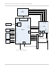
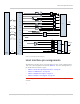
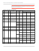
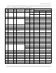
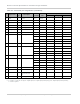
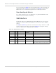
Table Of Contents
- Important Notice
- Safety and Hazards
- Limitation of Liability
- Patents
- Copyright
- Trademarks
- Contact Information
- Revision History
- 1: Introduction
- 2: Technology Overview
- 3: Standards Compliance
- 4: Electrical Specifications
- 5: RF Specifications
- 6: Power
- 7: Software Interface
- 8: Mechanical and Environmental Specifications
- 9: Regulatory and Industry Approvals
- A: Antenna Specification
- B: Design Checklist
- C: Testing
- D: Packaging
- E: References
- F: Acronyms
- Index

Product Technical Specification & Customer Design Guidelines
26 Proprietary and Confidential - Contents subject to change 2400074
Note: The following table describes the internal structure of the module.
GPIO pins are reserved for future use. For applications not requiring GPIO functionality,
leave these pins not connected on the host.
Table 4-1: Connector pin assignments
1
Pin Signal name
Pin
type
2
Description
Direction
to module
Active
state
Voltage levels (V)
Min Typ Max
1 NC - No connect
Reserved for future
use.
- - - - -
2 VCC V 3.3 V supply Input Power 3.0 3.3 3.6
3 NC - No connect
Reserved for future
use
- - - - -
4 GND V Ground Input Power - 0 -
5 NC - No connect
Reserved for future
use
- - - - -
6 GPIO1 - General purpose I/O Input high - 1.17 1.80 2.10
Input low - -0.3 - 0.63
Output high - 1.35 - 1.80
Output low - 0 - 0.45
7 NC - No connect - - - - -
8 USIM_PWR - SIM VCC supply Output Power 2.95 (3V SIM)
1.75 (1.8V SIM)
3.00 (3V SIM)
1.8 (1.8V SIM)
3.05 (3V SIM)
1.85 (1.8V SIM)
9 GND V Ground Input Power - 0 -
10 USIM_DATA - SIM IO pin Input Low -0.3 (3V SIM)
-0.3 (1.8V SIM)
- 1.05 (3V SIM)
0.63 (1.8V SIM)
High 1.95 (3V SIM)
1.17 (1.8V SIM)
3.0 (3V SIM)
1.8 (1.8V SIM)
3.3 (3V SIM)
2.1 (1.8V SIM)
Output Low 0 - 0.45
High 2.55 (3V SIM)
1.35 (1.8V SIM)
- 3.0 (3V SIM)
1.8 (1.8V SIM)
11 NC - No connect - - - - -
12 USIM_CLK - SIM Clock Output Low 0 - 0.45
High 2.55 (3V SIM)
1.35 (1.8V SIM)
- 3.0 (3V SIM)
1.8 (1.8V SIM)
13 NC - No connect - - - - -