
User's Manual

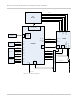
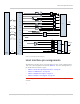
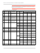
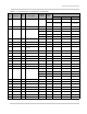
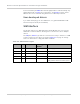
Table Of Contents
- Important Notice
- Safety and Hazards
- Limitation of Liability
- Patents
- Copyright
- Trademarks
- Contact Information
- Revision History
- 1: Introduction
- 2: Technology Overview
- 3: Standards Compliance
- 4: Electrical Specifications
- 5: RF Specifications
- 6: Power
- 7: Software Interface
- 8: Mechanical and Environmental Specifications
- 9: Regulatory and Industry Approvals
- A: Antenna Specification
- B: Design Checklist
- C: Testing
- D: Packaging
- E: References
- F: Acronyms
- Index

Electrical Specifications
Rev 4 Sep.11 Proprietary and Confidential - Contents subject to change 25
Figure 4-2: Expanded RF block diagram
Host interface pin assignments
The MC7750 host I/O connector provides pins for power, serial communications,
and control. Pin assignments are listed in
Tab l e 4-1. See the following tables for
pin details based on interface types:
• Tab l e 4-2, Power and ground specifications, on page 29
• Tab l e 4-3, USB interface, on page 29
• Tab l e 4-4, SIM interface signal, on page 30
• Tab l e 4-5, Module control signals, on page 33
Note: On any given interface (USB, SIM, etc.), leave unused inputs and outputs as no-
connects.
Diplexer
SP5T
DRX_LB2
B8
B8
PRX_LB1
BC0+B5+GSM850
B8+GSM900
PRX_LB2
PRX_MB2
PRX_MB1
DRX_MB1
B13
B13
DRX_LB1
DRX_MB2
DRX_HB
B1d
BC0/B5
GSM850/900
GSM1800/1900
TX_LB4
TX_MB1
TX_LB2
TX_LB1
TX_LB3
TX_MB3
RF Diversity/GPS
Connector 2
SP2T
GPS
LNA
GNSS
SP2T
PA
RF Main
Connector
SP10T
RTR8600
B1
BC1/B2
SP2T
PRX_I
D
R
X
_
Q
PRX_Q
D
R
X
_
I
BASEBAND:
MDM9600 or
PMIC8028
GNSS_I
GNSS_Q
TX_I
T
X
_
Q
Jammer Det
TCXO
DAC_REF
RTR_SSB
GNSS
Connector 1
B13d
BC1d + B2d
BC0d + B5d + B8d
Power Det
B1d
GSM1800 + GSM1900
TX_MB4
B1
BC1 + B2
BC0 + B5
B13
BC1/B2
B1
PA
PA
PA
PA
PA