
User's Manual

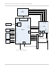
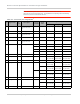
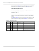
Table Of Contents
- Important Notice
- Safety and Hazards
- Limitation of Liability
- Patents
- Copyright
- Trademarks
- Contact Information
- Revision History
- 1: Introduction
- 2: Technology Overview
- 3: Standards Compliance
- 4: Electrical Specifications
- 5: RF Specifications
- 6: Power
- 7: Software Interface
- 8: Mechanical and Environmental Specifications
- 9: Regulatory and Industry Approvals
- A: Antenna Specification
- B: Design Checklist
- C: Testing
- D: Packaging
- E: References
- F: Acronyms
- Index

Product Technical Specification & Customer Design Guidelines
24 Proprietary and Confidential - Contents subject to change 2400074
Figure 4-1: System block diagram
External NAND
1Gb NAND
EBI2
GPIO55
GPIO56
GPIO57
PCB ID
GPIO65
GPIO66
GPIO67
GPIO68
GPIO69
GPIO70
HW Rev ID
HW_ID_0
HW_ID_1
HW_ID_2
HW_ID_3
HW_ID_4
HW_ID_5
PCB_ID_0
PCB_ID_1
PCB_ID_2
W_DISABLE_N
VCC_3.3V
GPIO_1
USIM
HS-
USB
GPIO25
GPIO24
GPIO23
MFG MODE
MFG_MODE0_N
MFG_MODE1_N
MFG_MODE2_N
GPIO_2
GPIO_3
GPIO_4
USIM
VPH/
VBAT
KPD_PWR_N
BATT_ID/MPP8
BATT_THERM/MPP7
WLAN_LED_N
GPIO102
PS_HOLD
GPIO8
PM_INT_N
MPM_GPIO_1
MPM_GPIO_2
PMIC_SSBI
TCXO_EN
RF + GRFC_GPIO
RF
BLOCK
MDM9600
PM8028
INTERFACE CONNECTOR
VGA_MONITOR
VGA_UMTS_MONITOR
MPP11
PWM_OUT
MPP4
PA_BOOST_EN
XTAL_19M_IN
XO_OUT_D0
XO_OUT_A0
VCTCXO_DFF
TCXO_RTR
VCTCXO
XO_OUT_EN
PM_INT_N
SSBI
Internal
64MB DDR
SDRAM
USIM
GPIO_5
GPIO_6