
User's Manual


220 www.xilinx.com PowerPC™ 405 Processor Block Reference Guide
1-800-255-7778 UG018 (v2.0) August 20, 2004
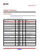
Appendix B: Signal Summary
R
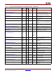
ISOCMDCRBRAMRDSELECT V-4 O ISOCM No
Connect
Select between even and odd
instruction words from DCR access
JTGC405BNDSCANTDO (INPUT) V-II Pro
and V-4
I JTAG 0 JTAG boundary scan input from the
previous boundary scan element TDO
output.
JTGC405TCK (INPUT) V-II Pro
and V-4
IJTAG1
(See
IEEE
1149.1)
JTAG TCK (test clock).
JTGC405TDI (INPUT) V-II Pro
and V-4
I JTAG 1 JTAG TDI (test-data in).
JTGC405TMS (INPUT) V-II Pro
and V-4
I JTAG 1 JTAG TMS (test-mode select).
JTGC405TRSTNEG (INPUT) V-II Pro
and V-4
IReset1
Required
Performs a JTAG test reset (TRST).
JTGC405TRSTNEG (INPUT) V-II Pro
and V-4
IJTAG1
Required
JTAG TRST
(test reset).
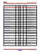
MCBCPUCLKEN (INPUT) V-II Pro
and V-4
I FPGA 1 Indicates the PowerPC 405 clock
enable should follow GWE during a
partial reconfiguration.
MCBJTAGEN (INPUT) V-II Pro
and V-4
I FPGA 1 Indicates the JTAG clock enable should
follow GWE during a partial
reconfiguration.
MCBTIMEREN (INPUT) V-II Pro
and V-4
I FPGA 1 Indicates the timer clock enable should
follow GWE during a partial
reconfiguration.
MCPPCRST (INPUT) V-II Pro
and V-4
I FPGA 1 Indicates the PowerPC 405 should be
reset when GSR is asserted during a
partial reconfiguration.
PLBC405DCUADDRACK (INPUT) V-II Pro
and V-4
I DSPLB 0 Indicates a PLB slave acknowledges
the current data-access request.
PLBC405DCUBUSY (INPUT) V-II Pro
and V-4
I DSPLB 0 Indicates the PLB slave is busy
performing an operation requested by
the DCU.
PLBC405DCUERR (INPUT) V-II Pro
and V-4
I DSPLB 0 Indicates an error was detected by the
PLB slave during the transfer of data to
or from the DCU.
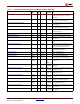
PLBC405DCURDDACK V-II Pro
and V-4
I DSPLB 0 Indicates the DCU read-data bus
contains valid data for transfer to the
DCU.
PLBC405DCURDDBUS[0:63] (INPUT) V-II Pro
and V-4
I DSPLB 0 The DCU read-data bus used to
transfer data from the PLB slave to the
DCU.
PLBC405DCURDWDADDR[1:3] (INPUT) V-II Pro
and V-4
I DSPLB 0 Indicates which word or doubleword
of an eight-word line transfer is
present on the DCU read-data bus.
PLBC405DCUSSIZE1 (INPUT) V-II Pro
and V-4
I DSPLB 0 Specifies the bus width (size) of the
PLB slave that accepted the request.
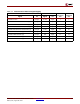
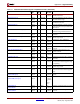
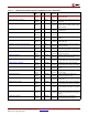
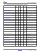
Table B-1: PowerPC 405 Interface Signals in Alphabetical Order (Continued)
Signal
FPGA
Type
a
I/O
Type
Interface
If Unused
Ties To:
b
Function