
User's Manual


184 www.xilinx.com PowerPC™ 405 Processor Block Reference Guide
1-800-255-7778 UG018 (v2.0) August 20, 2004
Chapter 4: PowerPC 405 APU Controller
R
The APU Controller serves two purposes: It performs clock domain synchronization
between the fast PowerPC clock and the slow FCM interface clock, and it can be configured
to decode certain FCM instructions. Depending on the FCM application, the APU
Controller can decode all instructions or no instructions at all, or decode some while the
FCM decodes others. A floating point unit (FPU) is an example of a good FCM candidate.
In the case of an FCM FPU, the APU Controller is capable of decoding all PowerPC floating
point instructions.
The FCM interface is a Xilinx adaptation of the native Auxiliary Processor Unit interface
implemented on the IBM processor core. The hard core APU Controller bridges the
PowerPC 405 APU interface and the external FCM interface.
FCM Instruction Processing
FCM instruction decoding can be done by the APU Controller or by the FCM, however, all
instruction execution is done in the FCM. There are two types of instructions that can be
executed by an FCM: pre-defined and user-defined (UDI). A pre-defined instruction has its
format defined by the PowerPC instruction set (for example, floating point), and the FCM
is simply a co-processor performing the ISA-defined execution. A user-defined instruction
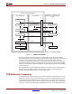
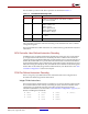
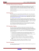
Figure 4-1: Pipeline Flow Diagram
Decode_Stage
PowerPC405 core
Virtex4 FX PowerPC405 block
Decode
Execute_Stage
Exe_Unit
load_reg
Writeback_Stage
Fabric Co-processor Module
(FCM)
FCM_Decode
FCM_Exe_Unit
UG018_04_01_040904
APU Controller
Instruction
Operands
Result
LoadData
APUC_Decode
LoadWB_Stage
Resynchronization_Interface