ML605 Hardware User Guide User Guide [optional] UG534 (v1.2.
Xilinx is disclosing this user guide, manual, release note, and/or specification (the "Documentation") to you solely for use in the development of designs to operate with Xilinx hardware devices. You may not reproduce, distribute, republish, download, display, post, or transmit the Documentation in any form or by any means including, but not limited to, electronic, mechanical, photocopying, recording, or otherwise, without the prior written consent of Xilinx.
Table of Contents Preface: About This Guide Guide Contents . . . . . . . . . . . . . . . . . . . . . . . . . . . . . . . . . . . . . . . . . . . . . . . . . . . . . . . . . . . . . . 5 Additional Documentation . . . . . . . . . . . . . . . . . . . . . . . . . . . . . . . . . . . . . . . . . . . . . . . . . . . 5 Additional Support Resources . . . . . . . . . . . . . . . . . . . . . . . . . . . . . . . . . . . . . . . . . . . . . . . . 6 Chapter 1: ML605 Evaluation Board Overview . . . . . . . . . . . . . .
FPGA_PROG_B Pushbutton SW4 (Active-Low) . . . . . . . . . . . . . . . . . . . . . . . . . . . . . . . SYSACE_RESET_B Pushbutton SW3 (Active-Low) . . . . . . . . . . . . . . . . . . . . . . . . . . . . System ACE CF CompactFlash Image Select DIP Switch S1 . . . . . . . . . . . . . . . . . . . . . . Mode, Osc Enable, Boot EEPROM Select, and Addr Select DIP Switch S2 . . . . . . . . . . . 19. VITA 57.1 FMC HPC Connector . . . . . . . . . . . . . . . . . . . . . . . . . . . . . . . . . . . . . . . . . 20.
Preface About This Guide This manual accompanies the Virtex®-6 FPGA ML605 Evaluation Board and contains information about the ML605 hardware and software tools. Guide Contents This manual contains the following chapters: • Chapter 1, “ML605 Evaluation Board,” provides an overview of the embedded development board and details the components and features of the ML605 board. • Appendix A, “Default Switch and Jumper Settings.” • Appendix B, “VITA 57.1 FMC LPC (J63) and HPC (J64) Connector Pinout.
Preface: About This Guide • Virtex-6 FPGA Memory Resources User Guide The functionality of the block RAM and FIFO are described in this user guide. • Virtex-6 FPGA SelectIO Resources User Guide This guide describes the SelectIO™ resources available in all Virtex-6 devices. • Virtex-6 FPGA GTX Transceivers User Guide This guide describes the GTX transceivers available in all Virtex-6 FPGAs except the XC6VLX760.
Chapter 1 ML605 Evaluation Board Overview The ML605 board enables hardware and software developers to create or evaluate designs targeting the Virtex®-6 XC6VLX240T-1FFG1156 FPGA. The ML605 provides board features common to many embedded processing systems. Some commonly used features include: a DDR3 SODIMM memory, an 8-lane PCI Express® interface, a tri-mode Ethernet PHY, general purpose I/O, and a UART.
Chapter 1: ML605 Evaluation Board Features The ML605 provides the following features: • 1. Virtex-6 XC6VLX240T-1FFG1156 FPGA • 2. 512 MB DDR3 Memory SODIMM • 3. 128 Mb Platform Flash XL • 4. 32 MB Linear BPI Flash • 5. System ACE CF and CompactFlash Connector • 6. USB JTAG • 7. Clock Generation • • 8 ♦ Fixed 200 MHz oscillator (differential) ♦ Socketed 2.5V oscillator (single-ended) ♦ SMA connectors (differential) ♦ SMA connectors for MGT clocking 8.
Overview • • • 16. Status LEDs ♦ Ethernet status ♦ FPGA INIT ♦ FPGA DONE ♦ System ACE CF Status 17. User I/O ♦ USER LED Group 1 - GPIO (8) ♦ USER LED Group 2 - directional (5) ♦ User pushbuttons - directional (5) ♦ CPU reset pushbutton ♦ User DIP switch - GPIO (8-pole) ♦ User SMA GPIO connectors (2) ♦ LCD character display (16 characters x 2 lines) 18.
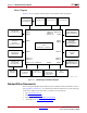
Chapter 1: ML605 Evaluation Board Block Diagram Figure 1-1 shows a high-level block diagram of the ML605 and its peripherals. X-Ref Target - Figure 1-1 JTAG USB Mini-B USB JTAG Circuit System ACE CF S.A. CompactFlash S.A. 8-bit MPU I/F VITA 57.
Detailed Description Detailed Description Figure 1-2 shows a board photo with numbered features corresponding to Table 1-1 and the section headings in this document.
Chapter 1: ML605 Evaluation Board Table 1-1: ML605 Features (Cont’d) Notes Schematic Page 200 MHz OSC, oscillator socket, SMA connectors 30 a. 200 MHz oscillator (on backside) Epson 200 MHz 2.5V LVDS OSC 30 b. Oscillator socket, singleended MMD Components 66 MHz 2.5V 30 c. SMA connectors SMA pair 30 d.
Detailed Description Table 1-1: ML605 Features (Cont’d) Number Feature Notes Switches 18 Schematic Page 13, 25, 39 a. Power On/Off Slide switch 39 b. FPGA_PROG_B pushbutton active-Low 13 c. System ACE CF Image Select 4-pole DIP switch (active-High) 25 d. Mode Switch 6-pole DIP switch (active-High) 25 19 FMC - HPC connector Samtec ASP-134486-01 16 -19 20 FMC - LPC connector Samtec ASP-134603-01 20 Power management a. PMBus controllers b.
Chapter 1: ML605 Evaluation Board The ML605 supports Master BPI-Up, JTAG, and Slave SelectMAP. These are selected by setting M[2:0] options 010, 101 and 110 shown in Table 1-2.
Detailed Description Table 1-3: Voltage Rails (Cont’d) U1 FPGA Bank I/O Rail Voltage Bank 24 VCC2V5_FPGA 2.5V Bank 25 VCC1V5_FPGA 1.5V Bank 26 VCC1V5_FPGA 1.5V Bank 32 VCC2V5_FPGA 2.5V Bank 33 VCC2V5_FPGA 2.5V Bank 34 VCC2V5_FPGA 2.5V Bank 35 VCC1V5_FPGA 1.5V Bank 36 VCC1V5_FPGA 1.5V Notes: 1. The VITA 57.1 specification stipulates that the Bank 12 voltage named FMC_VIO_B_M2C is supplied by the FMC card plugged onto the relevant FMC connector (ML605 J64).
Chapter 1: ML605 Evaluation Board Table 1-4: DDR3 SODIMM Connections (Cont’d) J1 SODIMM U1 FPGA Pin 16 Schematic Net Name Pin Number Pin Name A15 DDR3_A6 90 A6 B15 DDR3_A7 86 A7 G15 DDR3_A8 89 A8 F15 DDR3_A9 85 A9 M16 DDR3_A10 107 A10/AP M15 DDR3_A11 84 A11 H15 DDR3_A12 83 A12_BC_N J15 DDR3_A13 119 A13 D15 DDR3_A14 80 A14 C15 DDR3_A15 78 A15 K19 DDR3_BA0 109 BA0 J19 DDR3_BA1 108 BA1 L15 DDR3_BA2 79 BA2 J11 DDR3_D0 5 DQ0 E13 DDR3_D1 7 DQ1 F13
Detailed Description Table 1-4: DDR3 SODIMM Connections (Cont’d) J1 SODIMM U1 FPGA Pin ML605 Hardware User Guide UG534 (v1.2.
Chapter 1: ML605 Evaluation Board Table 1-4: DDR3 SODIMM Connections (Cont’d) J1 SODIMM U1 FPGA Pin 18 Schematic Net Name Pin Number Pin Name E24 DDR3_D54 174 DQ54 G25 DDR3_D55 176 DQ55 F28 DDR3_D56 181 DQ56 B31 DDR3_D57 183 DQ57 H29 DDR3_D58 191 DQ58 H28 DDR3_D59 193 DQ59 B30 DDR3_D60 180 DQ60 A30 DDR3_D61 182 DQ61 E29 DDR3_D62 192 DQ62 F29 DDR3_D63 194 DQ63 E11 DDR3_DM0 11 DM0 B11 DDR3_DM1 28 DM1 E14 DDR3_DM2 46 DM2 D19 DDR3_DM3 63 DM3 B22 DD
Detailed Description Table 1-4: DDR3 SODIMM Connections (Cont’d) J1 SODIMM U1 FPGA Pin Schematic Net Name Pin Number Pin Name C30 DDR3_DQS7_P 188 DQS7_P F18 DDR3_ODT0 116 ODT0 E17 DDR3_ODT1 120 ODT1 E18 DDR3_RESET_B 30 RESET_B K18 DDR3_S0_B 114 S0_B K17 DDR3_S1_B 121 S1_B D17 DDR3_TEMP_EVENT 198 EVENT_B B17 DDR3_WE_B 113 WE_B C17 DDR3_CAS_B 115 CAS_B L19 DDR3_RAS_B 110 RAS_B M18 DDR3_CKE0 73 CKE0 M17 DDR3_CKE1 74 CKE1 H18 DDR3_CLK0_N 103 CK0_N G18 D
Chapter 1: ML605 Evaluation Board 3. 128 Mb Platform Flash XL A 128 Mb Xilinx XCF128X-FTG64C Platform Flash XL device is used with an onboard 47 MHz oscillator (X4) to configure the FPGA in less than 100 ms from power valid as required by the PCI Express Card Electromechanical Specification. This allows the PCIe interface to be recognized and enumerated when plugged into a host PC.
Detailed Description ML605 Flash Boot Options The ML605 has two parallel wired flash memory devices as shown in Figure 1-3. At ML605 power-up, before FPGA configuration, DIP switch S2 switch 2 selects which flash device, U4 (BPI) or U27 (Platform Flash), provides the boot bitstream. Typically S2 switch 2 will be open/OFF to select the U27 Platform Flash.
Chapter 1: ML605 Evaluation Board Table 1-5: Platform Flash and BPI Flash Connections (Cont’d) U4 BPI Flash U1 FPGA Pin U27 Platform Flash Schematic Net Name Pin Number Pin Name Pin Number Pin Name AF24 FLASH_D0 34 DQ0 F2 DQ00 AF25 FLASH_D1 36 DQ1 E2 DQ01 W24 FLASH_D2 39 DQ2 G3 DQ02 V24 FLASH_D3 41 DQ3 E4 DQ03 H24 FLASH_D4 47 DQ4 E5 DQ04 H25 FLASH_D5 49 DQ5 G5 DQ05 P24 FLASH_D6 51 DQ6 G6 DQ06 R24 FLASH_D7 53 DQ7 H7 DQ07 G23 FLASH_D8 35 DQ8 E1 DQ0
Detailed Description FPGA Design Considerations for the Configuration Flash After FPGA configuration, the FPGA design can disable the configuration flash or access the configuration flash to read/write code or data. When the FPGA design does not use the configuration flash, the FPGA design must drive the FPGA FCS_B pin High in order to disable the configuration flash and put the flash into a quiescent, low-power state.
Chapter 1: ML605 Evaluation Board 5. System ACE CF and CompactFlash Connector The Xilinx System ACE CompactFlash (CF) configuration controller allows a Type I or Type II CompactFlash card to program the FPGA through the JTAG port. Both hardware and software data can be downloaded through the JTAG port. The System ACE CF controller supports up to eight configuration images on a single CompactFlash card.
Detailed Description Table 1-6 lists the System ACE CF connections.
Chapter 1: ML605 Evaluation Board 6. USB JTAG JTAG configuration is provided through onboard USB-to-JTAG configuration logic where a computer host accesses the ML605 JTAG chain through a Type-A (computer host side) to Type-Mini-B (ML605 side) USB cable. The JTAG chain of the board is illustrated in Figure 1-4. JTAG configuration is allowable at any time under any mode pin setting. JTAG initiated configuration takes priority over the mode pin settings.
Detailed Description The JTAG chain can be used to program the FPGA and access the FPGA for hardware and software debug. The JTAG connector (USB Mini-B J22) allows a host computer to download bitstreams to the FPGA using the Xilinx iMPACT software tool. In addition, the JTAG connector allows debug tools such as the ChipScope™ Pro Analyzer tool or a software debugger to access the FPGA. The iMPACT software tool can also program the BPI flash via the USB J22 connection.
Chapter 1: ML605 Evaluation Board X-Ref Target - Figure 1-7 Silkscreened outline has beveled corner Socket has notch in crossbar UG534_07_092109 Figure 1-7: ML605 Oscillator Socket Pin 1 Location Identifiers 28 www.xilinx.com ML605 Hardware User Guide UG534 (v1.2.
Detailed Description X-Ref Target - Figure 1-8 Oscillator body has one square corner Oscillator top has corner dot marking UG534_08_092109 Figure 1-8: ML605 Oscillator Pin 1 Location Identifiers SMA Connectors (Differential) A high-precision clock signal can be provided to the FPGA using differential clock signals through the onboard 50-ohm SMA connectors J58(P)/J55(N). ML605 Hardware User Guide UG534 (v1.2.1) January 21, 2010 www.xilinx.
Chapter 1: ML605 Evaluation Board GTX SMA Clock The ML605 includes a pair of SMA connectors for a GTX (MGT) Clock as described in Figure 1-9 and Table 1-7. X-Ref Target - Figure 1-9 C61 1 0.1UF 10V 2 X5R J30 32K10K-400E3 SMA_REFCLK_C_N1 SMA_REFCLK_N SMA_REFCLK_P GND1 GND2 GND3 SIG GND4 GND5 GND6 GND7 2 3 4 5 6 7 8 C62 1 0.
Detailed Description 8. Multi-Gigabit Transceivers (GTX MGTs) The ML605 provides access to 20 MGTs.
Chapter 1: ML605 Evaluation Board 9. PCI Express Endpoint Connectivity The 8-lane PCIe edge connector performs data transfers at the rate of 2.5 GT/s for a Gen1 application and 5.0 GT/s for a Gen2 application. The Virtex FPGA GTX MGTs are used for the multi-gigabit per second serial interfaces. The ML605 board trace impedance on all PCIe lanes supports both Gen1 and Gen2 applications. The ML605 supports up to Gen1 x8 and Gen2 x4 as shipped with a -1 speed grade for the LX240T device.
Detailed Description Table 1-8 shows the PCIe connector (P1) that provides up to 8-lane access through the GTX transceivers to the Virtex-6 FPGA integrated Endpoint block for PCIe designs.
Chapter 1: ML605 Evaluation Board Table 1-8: PCIe Edge Connector Connections (Cont’d) P1 PCIe Edge Connector U1 FPGA Pin Schematic Net Name AA3 Description Pin Number Pin Name PCIE_RX7_P B45 PETp7 AA4 PCIE_RX7_N B46 PETn7 P6 PCIE_100M_MGT0_P U14.16 Q0 P5 PCIE_100M_MGT0_N U14.15 NQ0 V6 PCIE_250M_MGT1_P U9.18 Q V5 PCIE_250M_MGT1_N U9.17 NQ U14.6 PCIE_CLK_QO_P A13 REFCLK+ U14.
Detailed Description References See the following websites for more Virtex-6 FPGA Integrated Endpoint Block for PCI Express information: • http://www.xilinx.com/products/ipcenter/V6_PCI_Express_Block.htm • http://www.xilinx.com/support/documentation/ipbusinterfacei-o_pciexpress_v6pciexpressendpointblock.htm In addition, see the PCI Express specifications for more information. [Ref 27] 10.
Chapter 1: ML605 Evaluation Board Table 1-10: SFP Module Connections P4 SFP Module Connector U1 FPGA Pin Schematic Net Name Pin Number Pin Name E3 SFP_RX_P 13 RDP_13 E4 SFP_RX_N 12 RDN_12 C3 SFP_TX_P 18 TDP_18 C4 SFP_TX_N 19 TDN_19 V23 SFP_LOS 8 LOS AP12 SFP_TX_DISABLE(1) 3 TX_DISABLE Notes: 1. The SFP TX Disable pin 3 is driven by transistor Q22, the base of which is driven by the FPGA signal SFP_TX_DISABLE_FPGA. 11.
Detailed Description Table 1-12: Board Connections for PHY Configuration Pins (Cont’d) Connection on Bit[2] Bit[1] Bit[0] Board Definition and Value Definition and Value Definition and Value Pin CFG5 VCC 2.5V DIS_FC = 1 DIS_SLEEP = 1 HWCFG_MD[3] = 1 CFG6 PHY_LED_RX SEL_BDT = 0 INT_POL = 1 75/50 OHM = 0 SGMII GTX Transceiver Clock Generation An Integrated Circuit Systems ICS844021I chip generates a high-quality, low-jitter, 125MHz LVDS clock from an inexpensive 25-MHz crystal oscillator.
Chapter 1: ML605 Evaluation Board Table 1-13: Ethernet PHYConnections (Cont’d) U80 M88E1111 U1 FPGA Pin Schematic Net Name Pin Number Pin Name AM12 PHY_RXD4 124 RXD4 AD11 PHY_RXD5 123 RXD5 AC12 PHY_RXD6 121 RXD6 AC13 PHY_RXD7 120 RXD7 AH12 PHY_TXC_GTXCLK 14 GTXCLK AD12 PHY_TXCLK 10 TXCLK AH10 PHY_TXER 13 TXER AJ10 PHY_TXCTL_TXEN 16 TXEN AM11 PHY_TXD0 18 TXD0 AL11 PHY_TXD1 19 TXD1 AG10 PHY_TXD2 20 TXD2 AG11 PHY_TXD3 24 TXD3 AL10 PHY_TXD4 25 TXD4 AM10
Detailed Description 12. USB-to-UART Bridge The ML605 contains a Silicon Labs CP2103GM USB-to-UART bridge device (U34) which allows connection to a host computer with a USB cable. The USB cable is supplied in this evaluation kit (Type A end to host computer, Type Mini-B end to ML605 connector J21). Table 1-14 details the ML605 J21 pinout. Xilinx UART IP is expected to be implemented in the FPGA fabric (for instance, Xilinx XPS UART Lite.
Chapter 1: ML605 Evaluation Board 13. USB Controller The ML605 provides USB support via a Cypress CY7C67300 EZ-Host™ Programmable Embedded USB Host and Peripheral Controller (U81). The host port is a USB Type-A connector (J5). A USB keyboard (without an internal USB hub) will be able to connect to this USB Host port to demonstrate functionality. The peripheral port is a USB Type MiniB (J20).
Detailed Description 14. DVI Codec The ML605 features a DVI connector (P3) to support an external video monitor. The DVI circuitry utilizes a Chrontel CH7301C (U38) capable of 1600 X 1200 resolution with 24-bit color. The video interface chip drives both the digital and analog signals to the DVI connector. A DVI monitor can be connected to the board directly. A VGA monitor can also be connected to the board using the supplied DVI-to-VGA adaptor.
Chapter 1: ML605 Evaluation Board 15. IIC Bus The ML605 implements four IIC bus interfaces at the FPGA.
Detailed Description X-Ref Target - Figure 1-14 U1 IIC_SDA_MAIN_LS FPGA IIC INTERFACE BANK 34 BANK 13 BANK 34 IIC_SCL_MAIN_LS IIC_SDA_SFP IIC_SCL_SFP IIC_SDA_DVI LEVEL SHIFTER IIC_SCL_DVI FMC_LPC_IIC_SDA_LS BANK 33 FMC_LPC_IIC_SCL_LS LEVEL SHIFTER J63 FMC LPC COLUMN C 2 Kb EEPROM on any FMC LPC Mezzanine Card Addr: 0b1010001 LEVEL SHIFTER LEVEL SHIFTER FMC_LPC_IIC_SCL FMC_LPC_IIC_SDA U6 ST MICRO M24C08-WDW6TP Addr: 0b1010100 through 0b1010111 J64 FMC HPC COLUMN C 2 Kb EEPROM on any FMC LPC Me
Chapter 1: ML605 Evaluation Board 8 Kb NV Memory The ML605 hosts an 8 Kb ST Microelectronics M24C08-WDW6TP IIC parameter storage memory device (U6). The IIC address of U7 is 0b1010100, and U6 is not write protected (WP pin 7 is tied to GND). The IIC memory is shown in Figure 1-15. X-Ref Target - Figure 1-15 VCC3V3 5% R414 0 5% 1/16W 2 1 2 1 2 R413 0 5% 1/16W IIC SCL MAIN IIC SDA MAIN 0 R414 1 VCC3V3 U6 6 SCL 5 SDA WP 1 A0 2 A1 3 A2 8 VCC GND 4 VCC3V3 7 1 C65 X5R 10V 0.
Detailed Description 16. Status LEDs Table 1-19 defines the status LEDs.
Chapter 1: ML605 Evaluation Board Ethernet PHY Status LEDs The Ethernet PHY status LEDs are mounted to be visible when the ML605 board is installed into a PC motherboard. They are mounted in right-angle, plastic housings and can be seen on the connector end of the board. This cluster of six LEDs is installed adjacent to the RJ45 Ethernet jack P2.
Detailed Description FPGA INIT and DONE LEDs The typical Xilinx FPGA power up and configuration status LEDs are present on the ML605. The red INIT LED DS31 comes on momentarily after the FPGA powers up and during its internal power-on process. The DONE LED DS13 comes on after the FPGA programming bitstream has been downloaded and the FPGA successfully configured. X-Ref Target - Figure 1-17 VCC2V5 VCC2V5 1 2 R419 330 5% 1/16W Q14 FPGA INIT B 2 FPGA_DONE 1 R3 27.
Chapter 1: ML605 Evaluation Board User LEDs The ML605 provides two groups of active-High LEDs as described in Figure 1-18 and Table 1-21. X-Ref Target - Figure 1-18 J62 GPIO_LED_0 GPIO_LED_1 1 2 GPIO_LED_2 GPIO_LED_3 3 4 GPIO_LED_4 GPIO_LED_5 5 6 GPIO_LED_6 7 GPIO_LED_7 8 1 2 1 2 2 2 1 R8 27.4 1% 1/16W 2 2 1 1 1 R11 27.4 1% 1/16W 2 LED-GRN-SMT DS12 2 2 1 R10 27.4 1% 1/16W LED-GRN-SMT DS11 2 1 R9 27.4 1% 1/16W LED-GRN-SMT DS9 1 DS10 2 1 1 1 R7 27.
Detailed Description Table 1-21: User LED Connections FPGA U1 Pin Schematic Net Name GPIO J62 Pin Controlled LED AC22 GPIO_LED_0 1 DS12 AC24 GPIO_LED_1 2 DS11 AE22 GPIO_LED_2 3 DS9 AE23 GPIO_LED_3 4 DS10 AB23 GPIO_LED_4 5 DS15 AG23 GPIO_LED_5 6 DS14 AE24 GPIO_LED_6 7 DS22 AD24 GPIO_LED_7 8 DS21 AP24 GPIO_LED_C – DS16 AD21 GPIO_LED_W – DS17 AE21 GPIO_LED_E – DS19 AH28 GPIO_LED_S – DS18 AH27 GPIO_LED_N – DS20 User Pushbutton Switches The ML605 provides
Chapter 1: ML605 Evaluation Board Table 1-22: User Pushbutton Switch Connections Pushbutton Switch Pin U1 FPGA Pin Schematic Net Name A19 GPIO_SW_N SW5.2 A18 GPIO_SW_S SW6.2 G17 GPIO_SW_E SW7.2 H17 GPIO_SW_W SW8.2 G26 GPIO_SW_C SW9.2 H10 CPU_RESET SW10.2 User DIP Switch The ML605 includes an active-High eight pole DIP switch as described in Figure 1-20 and Table 1-23. X-Ref Target - Figure 1-20 VCC1V5 SW1 16 15 14 13 12 11 10 9 1 2 3 4 5 6 7 8 5% SDMX-8-X 4.7K 2 4.
Detailed Description User SMA GPIO The ML605 includes an pair of SMA connectors for GPIO as described in Figure 1-21 and Table 1-24. X-Ref Target - Figure 1-21 J56 32K10K-400E3 2 GND1 3 GND2 4 GND3 1 5 SIG GND4 6 GND5 7 GND6 8 GND7 USER SMA GPIO N USER SMA GPIO P J76 32K10K-400E3 2 GND1 3 GND2 4 GND3 1 5 SIG GND4 6 GND5 7 GND6 8 GND7 UG534_21_072109 Figure 1-21: User SMA GPIO Table 1-24: User SMA Connections U1 FPGA Pin Schematic Net Name SMA Pin W34 USER_SMA_GPIO_N J56.
Chapter 1: ML605 Evaluation Board LCD Display (16 Character x 2 Lines) The ML605 board has a 16-character x 2-line LCD (Display Tech S162D BA BC, installed onto J41 2x7 header) on the board to display text information. Potentiometer R270 adjusts the contrast of the LCD. A ST2378E (U33) 2.5V-to-5V level-shifter is used to shift the voltage level between the FPGA and the LCD. The data interface to the LCD is connected to the FPGA to support 4-bit mode only.
Detailed Description 18. Switches The ML605 Evaluation board includes the following switches: • Power On/Off Slide Switch SW2 • FPGA_PROG_B SW4 (active-Low) • SYSACE_RESET_B SW3 (active-Low) • System ACE CF CompactFlash Image Select DIP Switch S1 (active-High) • MODE, Boot EEPROM Select and CCLK Osc Enable DIP switch S2 (active-High) Power On/Off Slide Switch SW2 SW2 is the ML605 board main power on/off switch.
Chapter 1: ML605 Evaluation Board FPGA_PROG_B Pushbutton SW4 (Active-Low) This switch grounds the FPGA's PROG_B pin when pressed. This action clears the FPGA. See the Virtex-6 FPGA Data Sheet for more information on clearing the contents of the FPGA. [Ref 4] X-Ref Target - Figure 1-24 RP4 1 4.
Detailed Description System ACE CF CompactFlash Image Select DIP Switch S1 System ACE CF CompactFlash (CF) image select DIP switch S1, switches 1–3, select which CF resident bitstream image is downloaded to the FPGA (Figure 1-26). S1 switches 1–3 offer eight binary addresses. When ON (High), the S1 switch 4 enables the System ACE CF controller to configure the FPGA from the CF card when a card is inserted or when the SYSACE RESET button is pressed. See “5.
Chapter 1: ML605 Evaluation Board Mode, Osc Enable, Boot EEPROM Select, and Addr Select DIP Switch S2 DIP switch S2 is a multi-purpose selector switch (Figure 1-27 and Table 1-27, page 57). FPGA Mode: S2 switches 3, 4, and 5 control the FPGA mode (Table 1-26). Oscillator Enable: S2 switch 1, CCLK_EXTERNAL, controls the enable pin of the 47 MHz oscillator SiT8102 (X4). When switch 1 is closed (CCLK_EXTERNAL High), X4 drives a 47 MHz clock onto the FPGA_CCLK signal.
Detailed Description Table 1-27: Switch S2 Configuration Details Switch Configuration Mode/Method Switch Net Name JTAG System ACE CF Slave SelectMAP Platform Flash XL Master BPI P30 Linear Flash S2.1 CCLK_EXTERNAL Off On Off S2.2 P30_CS_SEL On(1) Off On S2.3 FPGA_M0 On Off Off S2.4 FPGA_M1 Off On On S2.5 FPGA_M2 On On Off S2.6 FLASH_A23 Off Don't Care Off(2) Notes: 1. In JTAG mode, S2.2 is shown as ON for FPGA access to the P30 Linear Flash. Alternatively, set S2.
Chapter 1: ML605 Evaluation Board Note: The ML605 board VADJ voltage for the FMC HPC and LPC connectors (J64 and J63) is fixed at 2.5V (non-adjustable). The 2.5V rail cannot be turned off. The ML605 VITA 57.1 FMC interfaces are compatible with 2.5V mezzanine cards capable of supporting 2.5V VADJ. Table 1-28 shows the VITA 57.1 FMC HPC connections. The connector pinout is in Appendix B, “VITA 57.1 FMC LPC (J63) and HPC (J64) Connector Pinout.
Detailed Description Table 1-28: J64 FMC HPC Pin VITA 57.
Chapter 1: ML605 Evaluation Board Table 1-28: J64 FMC HPC Pin 60 VITA 57.
Detailed Description Table 1-28: J64 FMC HPC Pin VITA 57.1 FMC HPC Connections (Cont’d) Schematic Net Name U1 FPGA Pin J64 FMC HPC Pin Schematic Net Name U1 FPGA Pin J2 FMC_HPC_CLK3_M2C_P(2) U84.6 K4 FMC_HPC_CLK2_M2C_P(2) U83.6 J3 FMC_HPC_CLK3_M2C_N(2) U84.7 K5 FMC_HPC_CLK2_M2C_N(2) U83.
Chapter 1: ML605 Evaluation Board Table 1-29: Power Supply Voltages for HPC Connector Voltage Supply VADJ 62 Allowable Voltage Range No Pins Max Amps Tolerance Max Capacitive Load Fixed 2.5V 4 4 +/- 5% 1000 uF VIO_B_M2C 0-VADJ 2 1.15 +/- 5% 500 uF VREF_A_M2C 0-VADJ 1 1 mA +/- 2% 10 uF VREF_B_M2C 0-VIO_B_M2C 1 1 mA +/- 2% 10 uF 3P3VAUX 3.3V 1 20 mA +/- 5% 150 uF 3P3V 3.3V 4 3 +/- 5% 1000 uF 12P0V 12V 2 1 +/- 5% 1000 uF www.xilinx.
Detailed Description 20. VITA 57.1 FMC LPC Connector The ML605 implements both the High Pin Count (HPC, J64) and Low Pin Count (LPC, J63) connector options of VITA 57.1.1 FMC specification. This section discusses the FMC LPC J63 connector. The FMC standard calls for two connector densities: a High Pin Count (HPC) and a Low Pin Count (LPC) implementation. A common 10 x 40 position (400 pin locations) connector form factor is used for both versions.
Chapter 1: ML605 Evaluation Board Table 1-30 shows the VITA 57.1 FMC LPC connections. The connector pinout is in Appendix B, “VITA 57.1 FMC LPC (J63) and HPC (J64) Connector Pinout.” Any signal named FMC_LPC_xxxx that is wired between a U1 FPGA pin and some other device does not appear in this table.. Table 1-30: J63 FMC LPC Pin 64 VITA 57.
Detailed Description Table 1-30: J63 FMC LPC Pin VITA 57.
Chapter 1: ML605 Evaluation Board Onboard Power Regulation Figure 1-28 shows the ML605 onboard power supply architecture. The ML605 uses power solutions from Texas Instruments. X-Ref Target - Figure 1-28 12V PWR Jack J25/J60 Power Supply Linear Regulator TL1963 5.0V@1.5A max U8 Power Controller 1 UCD9240PFC VCC5 U24 Switching Module PTD08A020W 1.00V@20A max U42 VCCINT Switching Module PTD08A010W 2.50V@10A max U91 VCCAUX Switching Module PTD08A020W 2.
Detailed Description Table 1-31: Onboard Power System Devices Device Type Reference Designator Description Power Rail Net Name Power Rail Schematic Voltage Page UCD9240PFC U24 PMBus Controller - Core (Addr = 52) 35 PTD08A020W U42 20A 0.6V - 3.6V Adj. Switching Regulator VCCINT_FPGA 1.00V 36 PTD08A020W U43 20A 0.6V - 3.6V Adj. Switching Regulator VCC2V5_FPGA 2.50V 37 PTD08A010W U91 10A 0.6V - 3.6V Adj. Switching Regulator VCCAUX 2.
Chapter 1: ML605 Evaluation Board 22. System Monitor The System Monitor provides information regarding the FPGA on-chip temperature and power supply conditions via JTAG and an internal FPGA interface. The System Monitor can also be used to monitor external analog signals via 17 external analog input channels. For more information regarding this functionality, which is featured on every Virtex-6 family member, see http://www.xilinx.com/systemmonitor.
Detailed Description System Monitor Header (J35) Figure 1-30 shows the pinout for the System Monitor 12-pin header. The header provides user access to the analog power supply (AVdd) and the 1.25V reference shown in Figure 1-29, page 68. Access to the FPGA thermal diode and dedicated analog input channel (Vp/Vn) is also provided on this header. The header can be used to connect user specific analog signals and sensors to the system monitor.
Chapter 1: ML605 Evaluation Board ML605 Board Power Monitor In addition to monitoring the FPGA core supply power consumption, two auxiliary analog input channels (of the 16 that are available) are used to implement a power monitor for the entire ML605 board. The board power is monitored at the 12V power input connector. Figure 1-31 shows how the power monitor is implemented and connected to the System Monitor auxiliary input channels 12 and 13.
Detailed Description Fan Controller In highly demanding situations, active thermal management in the form of a heat sink and fan may be required. In order to support this, drive circuitry for an external fan has been provided on the ML605. A fan with tach output can be connect at header J59 as shown in Figure 1-32. The fan PWM signal is generated by the FPGA and the tach input can be used to close the control loop and regulate the fan speed.
Chapter 1: ML605 Evaluation Board FPGA Power Supply Margining The PMBus (IIC), which provides access to the 2 x UDC9240 power controllers, can also be accessed via FPGA I/O in addition to a dedicated header (J3), see Figure 1-33. A full description of the UDC9240 functionality is outside the scope of this user guide. However, this useful feature can be used, for example, to margin the FPGA and board power supplies when evaluating a design.
Configuration Options Configuration Options The FPGA on the ML605 Evaluation Board can be configured by the following methods: • “3. 128 Mb Platform Flash XL,” page 20 • “4. 32 MB Linear BPI Flash,” page 20 • “5. System ACE CF and CompactFlash Connector” • “6. USB JTAG,” page 26 For more information, see the Virtex-6 FPGA Configuration User Guide at http://www.xilinx.com/support/documentation/user_guides/ug360.pdf.
Chapter 1: ML605 Evaluation Board 74 www.xilinx.com ML605 Hardware User Guide UG534 (v1.2.
Appendix A Default Switch and Jumper Settings Table A-1: Default Switch Settings REFDES SW2 Function/Type Board power slide-switch Default off User GPIO 8-pole DIP switch SW1 8 off 7 off 6 off 5 off 4 off 3 off 2 off 1 off System ACE CF configuration and image select 4-pole DIP switch S1 4 SysACE Mode = 1 (1) off 3 SysAce CFGAddr 2 = 0 off 2 SysAce CFGAddr 1 = 0 off 1 SysAce CFGAddr 0 = 0 off FPGA mode, boot PROM select and FPGA CCLK select 6-pole DIP switch S2 6 FLA
Appendix A: Default Switch and Jumper Settings Table A-2: Default Jumper Settings Jumper REFDES Function Default J69 System ACE CF Error LED Enable Jump 1-2 J66 pins 1-2: GMII/MII to Cu pins 2-3: SGMII to Cu, no clk Jump 1 - 2 J67 pins 1-2: GMII/MII to Cu pins 2-3: SGMII to Cu, no clk Jump 1 - 2 J68 J66 pins 1-2, J68 ON: RGMII, modified MII in Cu no jumper J18 exclude FMC LPC connector Jump 1 - 2 J17 exclude FMC LPC connector Jump 1 - 2 J19 Test_mon_vrefp sourced by U23, REF3012 Ju
Appendix B VITA 57.1 FMC LPC (J63) and HPC (J64) Connector Pinout Figure B-1 shows the pinout of the FMC LPC connector. Pins marked NC are not connected.
1 2 3 4 5 6 7 8 9 10 11 12 13 14 15 16 17 18 19 20 21 22 23 24 25 26 27 28 29 30 31 32 33 34 35 36 37 38 39 40 K VR EF _B _M2C GND GND CLK2_M2C _P CLK2_M2C _N GND HA02_P HA02_N GND HA06_P HA06_N G ND HA10_P HA10_N G ND HA17_P _C C HA17_N_C C G ND HA21_P HA21_N G ND HA23_P HA23_N G ND HB00_P _C C HB00_N_C C G ND HB06_P _C C HB06_N_C C G ND HB10_P HB10_N G ND HB14_P HB14_N G ND HB17_P _C C HB17_N_C C G ND V IO_B _M2C J GND C LK 3_M2C_P C LK 3_M2C_N GND GND HA03_P HA03_N GND HA07_P HA07_N GND HA11_P HA11_N G
Appendix C ML605 Master UCF The UCF template is provided for designs that target the ML605. Net names provided in the constraints below correlate with net names on the ML605 Rev. D schematic. On identifying the appropriate pins, the net names below should be replaced with net names in the user RTL. See the Constraints Guide for more information.
Appendix C: ML605 Master UCF NET NET NET NET NET NET NET NET NET NET NET NET NET NET NET NET NET NET NET NET NET NET NET NET NET NET NET NET NET NET NET NET NET NET NET NET NET NET NET NET NET NET NET NET NET NET NET NET NET NET NET NET NET NET NET NET NET NET NET NET NET NET NET NET NET 80 "DDR3_D8" "DDR3_D9" "DDR3_D10" "DDR3_D11" "DDR3_D12" "DDR3_D13" "DDR3_D14" "DDR3_D15" "DDR3_D16" "DDR3_D17" "DDR3_D18" "DDR3_D19" "DDR3_D20" "DDR3_D21" "DDR3_D22" "DDR3_D23" "DDR3_D24" "DDR3_D25" "DDR3_D26" "DDR3_D27"
NET NET NET NET NET NET NET NET NET NET NET NET NET NET NET NET NET NET NET NET NET NET NET ## NET NET NET NET NET NET NET NET NET NET NET NET NET NET NET NET NET NET NET ## NET NET NET NET NET NET NET NET NET NET NET NET NET NET NET NET NET NET NET NET NET "DDR3_DQS0_P" "DDR3_DQS1_N" "DDR3_DQS1_P" "DDR3_DQS2_N" "DDR3_DQS2_P" "DDR3_DQS3_N" "DDR3_DQS3_P" "DDR3_DQS4_N" "DDR3_DQS4_P" "DDR3_DQS5_N" "DDR3_DQS5_P" "DDR3_DQS6_N" "DDR3_DQS6_P" "DDR3_DQS7_N" "DDR3_DQS7_P" "DDR3_ODT0" "DDR3_ODT1" "DDR3_RAS_B" "DDR3_
Appendix C: ML605 Master UCF NET NET NET NET NET NET NET NET NET NET NET NET NET NET NET NET NET NET NET NET NET NET NET NET NET ## ## NET NET NET NET NET NET NET NET NET NET NET NET NET NET NET NET NET NET NET NET NET NET NET NET NET NET NET NET NET NET NET NET NET NET NET NET NET NET 82 "FLASH_A21" "FLASH_A22" "FLASH_A23" "FLASH_D0" "FLASH_D1" "FLASH_D2" "FLASH_D3" "FLASH_D4" "FLASH_D5" "FLASH_D6" "FLASH_D7" "FLASH_D8" "FLASH_D9" "FLASH_D10" "FLASH_D11" "FLASH_D12" "FLASH_D13" "FLASH_D14" "FLASH_D15" "
NET NET NET NET NET NET NET NET NET NET NET NET NET NET NET NET NET NET NET NET NET NET NET NET NET NET NET NET NET NET NET NET NET NET NET NET NET NET NET NET NET NET NET NET NET NET NET NET NET NET NET NET NET NET NET NET NET NET NET NET NET NET NET NET NET "FMC_HPC_DP6_M2C_N" "FMC_HPC_DP6_M2C_P" "FMC_HPC_DP7_C2M_N" "FMC_HPC_DP7_C2M_P" "FMC_HPC_DP7_M2C_N" "FMC_HPC_DP7_M2C_P" "FMC_HPC_GBTCLK0_M2C_N" "FMC_HPC_GBTCLK0_M2C_P" "FMC_HPC_GBTCLK1_M2C_N" "FMC_HPC_GBTCLK1_M2C_P" "FMC_HPC_HA00_CC_N" "FMC_HPC_HA00_C
Appendix C: ML605 Master UCF NET NET NET NET NET NET NET NET NET NET NET NET NET NET NET NET NET NET NET NET NET NET NET NET NET NET NET NET NET NET NET NET NET NET NET NET NET NET NET NET NET NET NET NET NET NET NET NET NET NET NET NET NET NET NET NET NET NET NET NET NET NET NET NET NET 84 "FMC_HPC_HB03_P" "FMC_HPC_HB04_N" "FMC_HPC_HB04_P" "FMC_HPC_HB05_N" "FMC_HPC_HB05_P" "FMC_HPC_HB06_CC_N" "FMC_HPC_HB06_CC_P" "FMC_HPC_HB07_N" "FMC_HPC_HB07_P" "FMC_HPC_HB08_N" "FMC_HPC_HB08_P" "FMC_HPC_HB09_N" "FMC_HP
NET NET NET NET NET NET NET NET NET NET NET NET NET NET NET NET NET NET NET NET NET NET NET NET NET NET NET NET NET NET NET NET NET NET NET NET NET NET ## NET NET NET NET NET NET NET NET NET NET NET NET NET NET NET NET NET NET NET NET NET NET NET NET NET NET "FMC_HPC_LA16_N" "FMC_HPC_LA16_P" "FMC_HPC_LA17_CC_N" "FMC_HPC_LA17_CC_P" "FMC_HPC_LA18_CC_N" "FMC_HPC_LA18_CC_P" "FMC_HPC_LA19_N" "FMC_HPC_LA19_P" "FMC_HPC_LA20_N" "FMC_HPC_LA20_P" "FMC_HPC_LA21_N" "FMC_HPC_LA21_P" "FMC_HPC_LA22_N" "FMC_HPC_LA22_P" "F
Appendix C: ML605 Master UCF NET "FMC_LPC_LA07_N" NET "FMC_LPC_LA07_P" NET "FMC_LPC_LA08_N" NET "FMC_LPC_LA08_P" NET "FMC_LPC_LA09_N" NET "FMC_LPC_LA09_P" NET "FMC_LPC_LA10_N" NET "FMC_LPC_LA10_P" NET "FMC_LPC_LA11_N" NET "FMC_LPC_LA11_P" NET "FMC_LPC_LA12_N" NET "FMC_LPC_LA12_P" NET "FMC_LPC_LA13_N" NET "FMC_LPC_LA13_P" NET "FMC_LPC_LA14_N" NET "FMC_LPC_LA14_P" NET "FMC_LPC_LA15_N" NET "FMC_LPC_LA15_P" NET "FMC_LPC_LA16_N" NET "FMC_LPC_LA16_P" NET "FMC_LPC_LA17_CC_N" NET "FMC_LPC_LA17_CC_P" NET "FMC_LPC_L
NET NET NET NET NET NET NET NET ## NET NET NET NET NET NET NET NET ## NET NET NET NET NET NET NET NET ## NET NET NET NET NET ## NET NET NET NET NET ## NET NET NET NET NET NET ## NET NET NET NET NET NET NET ## NET ## NET NET NET NET NET NET NET NET NET "FPGA_M0" "FPGA_M1" "FPGA_M2" "FPGA_PROG_B" "FPGA_TCK" "FPGA_TDI" "FPGA_TMS" "FPGA_VBATT" LOC LOC LOC LOC LOC LOC LOC LOC = = = = = = = = "U8"; "W8"; "V8"; "L8"; "AE8"; "AD8"; "AF8"; "N8"; ## ## ## ## ## ## ## ## 3 4 4 1 80 82 85 1 on on on on on on on
Appendix C: ML605 Master UCF NET "PCIE_RX2_N" NET "PCIE_RX2_P" NET "PCIE_RX3_N" NET "PCIE_RX3_P" NET "PCIE_RX4_N" NET "PCIE_RX4_P" NET "PCIE_RX5_N" NET "PCIE_RX5_P" NET "PCIE_RX6_N" NET "PCIE_RX6_P" NET "PCIE_RX7_N" NET "PCIE_RX7_P" NET "PCIE_TX0_N" NET "PCIE_TX0_P" NET "PCIE_TX1_N" NET "PCIE_TX1_P" NET "PCIE_TX2_N" NET "PCIE_TX2_P" NET "PCIE_TX3_N" NET "PCIE_TX3_P" NET "PCIE_TX4_N" NET "PCIE_TX4_P" NET "PCIE_TX5_N" NET "PCIE_TX5_P" NET "PCIE_TX6_N" NET "PCIE_TX6_P" NET "PCIE_TX7_N" NET "PCIE_TX7_P" NET "P
NET ## NET NET NET NET NET NET ## NET NET NET NET NET NET ## NET NET NET NET NET NET ## NET NET ## NET NET NET NET NET NET NET NET NET NET NET NET NET NET NET NET NET NET NET NET NET ## NET NET ## NET NET NET NET ## NET NET NET NET NET NET NET NET NET "PMBUS_DATA_LS" LOC = "AB10"; ## 2 on Q17 "SFP_LOS" "SFP_RX_N" "SFP_RX_P" "SFP_TX_DISABLE_FPGA" "SFP_TX_N" "SFP_TX_P" LOC LOC LOC LOC LOC LOC = = = = = = "V23"; "E4"; "E3"; "AP12"; "C4"; "C3"; ## ## ## ## ## ## 8 12 13 1 19 18 on on on on on on P4
Appendix C: ML605 Master UCF NET NET NET NET NET NET NET NET NET NET NET NET NET NET ## NET NET NET NET NET ## NET NET NET NET 90 "USB_D6_LS" "USB_D7_LS" "USB_D8_LS" "USB_D9_LS" "USB_D10_LS" "USB_D11_LS" "USB_D12_LS" "USB_D13_LS" "USB_D14_LS" "USB_D15_LS" "USB_INT_LS" "USB_RD_B_LS" "USB_RESET_B_LS" "USB_WR_B_LS" LOC LOC LOC LOC LOC LOC LOC LOC LOC LOC LOC LOC LOC LOC = = = = = = = = = = = = = = "V27"; "U25"; "Y28"; "W32"; "W31"; "Y29"; "W29"; "Y34"; "Y33"; "Y31"; "Y27"; "W25"; "T25"; "V25"; ## ## ##
Appendix D References This section provides references to documentation supporting Virtex-6 FPGAs, tools, and IP. For additional information, see www.xilinx.com/support/documentation/index.htm. Documents supporting the ML605 Evaluation Board: 1. UG535, ML605 Reference Design User Guide 2. UG525, Getting Started with the Xilinx Virtex-6 FPGA ML605 Evaluation Kit 3. DS150, Virtex-6 Family Overview 4. DS152, Viretx-6 FPGA Data Sheet: DC and Switching Characteristics 5.
Appendix D: References Additional documentation: 22. Micron Technology, Inc., DDR3 SODIMM Specification (MT4JSF6464HY-1G1) 23. Winbond, Serial Flash Memory Data Sheet (W25Q64VSFIG) 24. Numonyx, Embedded Flash Memory Data Sheet (TE28F128J3D-75) 25. Epson Toyocom, Oscillator Data Sheet (EG-2121CA-200.0000M-LHPA) 26. MMD Components, MBH Series Data Sheet (MBH2100H-66.000 MHz) 27. PCI SIG, PCI Express Specifications 28. Marvell, Alaska Gigabit Ethernet Transceivers Product Page 29.