0 PLB PCI Full Bridge (v1.00a) DS508 March 21, 2006 0 Product Specification 0 Introduction LogiCORE™ Facts Supported Device Family Virtex™-II Pro, Virtex-4 plb_pci Resources Used Virtex-IIP Min Max 49 50 I/O (PLB-related) 397 433 LUTs 3350 3870 2570 2970 8 8 I/O (PCI) FFs Block RAMs Host bridge functionality (often called North bridge functionality) is an optional functionality. Configuration Read and Write PCI commands can be performed from the PLB-side of the bridge.
PLB PCI Full Bridge (v1.00a) Features • Independent PLB and PCI clocks • 33 MHz, 32-bit PCI bus support • Utilizes two pairs of FIFOs to exploit the separate master and slave PLB IPIF modules. • Includes a master IP module for remote PCI initiator transactions, which follows the protocol for interfacing with the master IPIF module utilizing Xilinx LocalLink protocol. The PLB PCI Bridge translates the PCI initiator request to PLB IPIF master transactions.
PLB PCI Full Bridge (v1.00a) default in all transfers. Address translation is performed by high-order bit substitution.
PLB PCI Full Bridge (v1.00a) System Reset When the bridge is reset, both RST_N and PLB_reset must be simultaneously held at reset for at least twenty clock periods of the slowest clock. Evaluation Version The PLB PCI Bridge is delivered with a hardware evaluation license. When programmed into a Xilinx device, the core will function in hardware for about 8 hours at the typical frequency of operation. To use the PLB PCI Bridge without this timeout limitation, a full license must be purchased.
PLB PCI Full Bridge (v1.00a) core. These documents detail the v3.0 core operation, including configuration cycles, and are available from Xilinx. As required by the LogiCORE v3.0 core, GNT_N must be asserted for two clock cycles to initiate a PCI transaction by the PLB PCI Bridge. Bus Interface Parameters Because many features in the IPIF v3.
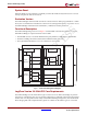
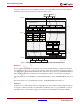
PLB PCI Full Bridge (v1.00a) Example 3 outlines the use of the PCIBAR parameter sets for the address translation of PCI addresses within the range of a given PCIBAR to a remote PLB address space. Figure Top x-ref 2 BAR_10 BAR_11 PLB Bus PLB PCI Full Bridge IPIF C_IPIFBAR_NUM = 3 IPIFBAR_1 IPIFBAR_2 (high-order bit sub) (high-order bit sub) (high-order bit sub) Addr to PCI Addr to PCI Addr to PCI IPIFBAR_3 IPIFBAR_4 IPIFBAR_5 IPIF to v3.
PLB PCI Full Bridge (v1.00a) As in example 1, it is assumed that the parameter C_INCLUDE_BAROFFSET_REG=0, therefore the C_IPIFBAR2PCIBAR_N parameters define the address translation.
PLB PCI Full Bridge (v1.00a) Accessing the PLB PCI Bridge PCIBAR_1 with address 0x1235FEDC on the PCI bus yields 0xFE35FEDC on the PLB bus.
PLB PCI Full Bridge (v1.
PLB PCI Full Bridge (v1.
PLB PCI Full Bridge (v1.00a) Table 1: PLB PCI Bridge Interface Design Parameters (Contd) Allowable Values Default Value VHDL Type C_TRIG_IPIF_ WRBURST_ OCC_LEVEL 2 to the lesser of 24 or the PCI2IPIF FIFO DEPTH-3. PCI2IPIF FIFO DEPTH given by 2^C_PCI2IPIF_FIFO_A BUS_WIDTH 8 integer C_TRIG_PCI_ DATA_XFER_ OCC_LEVEL 2 to the lesser of 24 or the IPIF2PCI FIFO DEPTH-3. IPIF2PCI FIFO DEPH given by 2^C_IPIF2PCI_FIFO_ ABUS_WIDTH 8 integer 2 to the lesser of 24 or the IPIF2PCI FIFO DEPTH-3.
PLB PCI Full Bridge (v1.00a) Table 1: PLB PCI Bridge Interface Design Parameters (Contd) G51 Includes IDELAY primitive on GNT_N. Set by tcl-scripts and ignored if not Virtex-4. G52 Provides a means for BSB to pass LOC coordinates for IDELAYCTRLs for a given board to EDK and is optional for user to set LOC constraints. This parameter has no impact on bridge functionality.
PLB PCI Full Bridge (v1.00a) Table 1: PLB PCI Bridge Interface Design Parameters (Contd) Generic Feature / Description Parameter Name Allowable Values Default Value VHDL Type G61 Include configuration functionality via IPIF transactions C_INCLUDE_ PCI_CONFIG 0 = Not included 1 = Included 1 integer G62 Number of IDSEL signals supported C_NUM_ IDSEL 1 to 16 8 integer G63 PCI address bit that PCI v3.
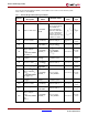
PLB PCI Full Bridge (v1.00a) PLB PCI Bus Interface I/O Signals The I/O signals for the PLB PCI Bridge are listed in Table 2. The interfaces referenced in this table are shown in Figure 1 in the PLB PCI Bridge block diagram. Table 2: PLB PCI Bridge I/O Signals Port Signal Name Interface I/O Description System Signals P1 IP2INTC_Irpt Internal O Interrupt from IP to the Interrupt Controller PLB Signals PLB_Clk PLB Bus I PLB main bus clock. See table note 1.
PLB PCI Full Bridge (v1.
PLB PCI Full Bridge (v1.
PLB PCI Full Bridge (v1.
PLB PCI Full Bridge (v1.00a) Port and Parameter Dependencies The dependencies between the IPI v3.0 Bridge design port (i.e., I/O signals) and parameters are shown in Table 1.
PLB PCI Full Bridge (v1.00a) Table 3: PLB PCI Bridge Parameters-Port Dependencies (Contd) Affects Depends Description Meaningful only if G48 = 0 and G1>2. In this case only high-order bits that are the same in G10 and G11 are meaningful.
PLB PCI Full Bridge (v1.00a) Table 3: PLB PCI Bridge Parameters-Port Dependencies (Contd) Generic Parameter Depends Description The set of PCI/v3.0 BAR-parameters of N = 0 to C_PCIBAR_NUM-1 are meaningful and the parameters of N = C_PCIBAR_NUM up to and including 2 have no effect. If C_PCIBAR_NUM = 3, the set of PCI/v3.0 BAR-parameters of N = 0 to 2 are all meaningful (i.e.
PLB PCI Full Bridge (v1.
PLB PCI Full Bridge (v1.00a) Table 3: PLB PCI Bridge Parameters-Port Dependencies (Contd) G62 C_NUM_IDSEL G63 C_BRIDGE_IDSEL_ADDR _BIT Affects Depends Description G49 and G63 G61 and G63 If G61=0, G62 has no meaning. If G61=1, G62 sets the number of devices supported in configuration operations. Must be sufficiently large to include the address bit defined by G63.
PLB PCI Full Bridge (v1.00a) Table 4: Supported PCI Bus Commands 1101 Dual Address Cycle Ignore No 1110 Memory Read Line Yes No 1111 Memory Write Invalidate Yes No PLB PCI Bridge Register Descriptions S The PLB PCI Bridge contains addressable registers for read/write operations as shown in Table 5. The base address for these registers is set by the base address parameter (C_BASEADDR). The address of each register is then calculated by an offset to the base address as shown in Table 5.
PLB PCI Full Bridge (v1.00a) Register and Parameter Dependencies The addressable registers in the PLB PCI Bridge depend on the parameter settings shown in Table 6.
PLB PCI Full Bridge (v1.00a) Global Interrupt Enable Register Description A global enable is provided to globally enable or disable interrupts from the PCI device. This bit is AND’d with the output to the interrupt controller. Bit assignment is shown in Table 7. Unlike most other registers, this bit is the MSB on the PLB. This bit is read/write and cleared upon reset.
PLB PCI Full Bridge (v1.00a) Table 8: Bridge Interrupt Register Bit Definitions (Bit Assignment Assumes 32-bit Bus) (Contd) Bit(s) Name Access Reset Value Description 25 PLB Master Write Master Abort Read/Write 1 to clear 0x0 PLB Master Write Master Abort- Interrupt(25) indicates that the PLB PCI Bridge asserted a PCI master abort due to no response from a target.
PLB PCI Full Bridge (v1.00a) Table 9: Bridge Interrupt Enable Register Bit Definitions (Bit assignment assumes 32-bit bus) (Contd) 27 PLB Master Write PERR 28 PLB Master Write SERR 29 PLB Master Read Target Abort 0x0 PLB Master Write Retry Enable- Enables this interrupt to be passed to the interrupt controller. • 0 - Not enabled. • 1 - Enabled. 0x0 PLB Master Write Master Abort Enable- Enables this interrupt to be passed to the interrupt controller. • 0 - Not enabled. • 1 - Enabled.
PLB PCI Full Bridge (v1.00a) Configuration Address Port Register Description The Configuration Address Port Register exists only if the bridge is configured with PCI host bridge configuration functionality (i.e., C_INCLUDE_PCI_CONFIG=1). This register is read/write with some bits hardwired as in Table 10. Definition of this register is a subset of the PCI 2.2. All accesses to the register are 32-bit accesses. Data is latched on a write in all 32-bits except where bits are hard-wired.
PLB PCI Full Bridge (v1.00a) bus number. The highest subordinate bus number is also an 8-bit value. The fields are defined in Table 12. Reset clears all bits.
PLB PCI Full Bridge (v1.00a) The example below shows how the IPIFBAR2PCIBAR_N registers assignments define translation of PLB addresses within the range of a given IPIFBAR to PCI address space. Setting C_INCLUDE_BAROFFSET_REG=1 includes high-order bit registers for all IPIFBARs defined by C_IPIFBAR_NUM. In this example where C_IPIFBAR_NUM=4, the following assignments for each range are made.
PLB PCI Full Bridge (v1.00a) Writing 0xFEDC0000 to IPIFBAR2PCIBAR_1 High-Order Bit Register and then accessing the PLB PCI bridge IPIFBAR_1 with address 0xABCDF123 on the PLB bus would yield 0xFEDC1123 on the PCI bus. Writing 0x40000000 to IPIFBAR2PCIBAR_2 High-Order Bit Register and then accessing the PLB PCI bridge IPIFBAR_2 with address 0xFFFEDCBA on the PLB bus would yield 0x41FEDCBA on the PCI bus.
PLB PCI Full Bridge (v1.00a) PLB PCI Transactions The following subsections discuss details of the following types of transactions for the PLB PCI bridge to realize data throughputs as high as 132 MB/sec. This assumes the PLB clock is 100 MHz or higher. Lower data rates will be realized with lower PLB clock rates for some transactions. • The section, PLB Master Initiates a Read Request of a PCI target, discusses the PLB master read of a PCI target where the v3.0 core is the PCI initiator.
PLB PCI Full Bridge (v1.00a) Table 15: Translation Table for PLB transactions to PCI commands (Contd) Sequential Read, 4, 8 and 16-word cacheline read (1) I/O Read Memory Read Multiple Not Supported Single Write (<=8 bytes) I/O Write Memory Write Not Supported Write Burst transfer double word I/O Write Memory Write (multiple data phase) Not Supported Sequential fill, 4, 8 and 16-word cacheline write (2) I/O Write Memory Write (multiple data phase) Not Supported Notes: 1.
PLB PCI Full Bridge (v1.00a) • Address translations in both directions are performed by high-order address bits substitution in the address vector before crossing to the other bus domain. Byte addressing integrity is maintained between buses. ES S • The user’s system must be designed to accomodate certain restrictions on throttling by the PLB PCI Bridge.
PLB PCI Full Bridge (v1.00a) mode). • If the PCI target address space is IO-space, the 2 LSBs are passed unchanged from that presented on the PLB bus. If the PLB transaction is not a burst (i.e., PLB_rdBurst is not high), a single PCI transaction (I/O or Memory Read command) is performed and the PLB transaction is terminated on the first double word transaction. This results in low data throughput. S If the transaction is a PLB burst transaction (i.e.
PLB PCI Full Bridge (v1.00a) • If a SERR occurs during a valid data phase on a burst transfer, the PLB PCI Bridge causes an IPIF timeout and asserts the IPIF Master Read SERR interrupt. SERR error on data phase could occur on the first PCI transaction or on a subsequent transaction due to an abnormal disconnect that allowed automatic reissue of the PCI read command. Most of the data transferred prior to the SERR assertion will be transferred.
PLB PCI Full Bridge (v1.00a) Table 17 summarizes the abnormal conditions with which a PCI target can respond and how the response is translated to the PLB master. Table 17: Response of PLB Master/v3.
PLB PCI Full Bridge (v1.00a) when an incomplete PCI transactions occur or when PCI errors occur. Details of the abnormal terminations are discussed in a later section. In these transactions, the v3.0 core is the PCI initiator. S The operation is essentially the same whether the PCI space is memory or I/O space; the only difference is the command sent to the v3.0 core by the PLB PCI Bridge. The bridge can accept both fixed length and arbitrary length burst transactions on the PLB.
PLB PCI Full Bridge (v1.00a) burst write data from the PLB to PCI beyond the valid IPIF BAR address range. The PLB PCI Bridge does not support fast back-to-back PCI transactions. Abnormal Terminations In the context of the PLB PCI bridge, cacheline transactions are special cases of a burst. Abnormal terminations during a cacheline write operation have the same response as a burst write transaction.
PLB PCI Full Bridge (v1.00a) transaction. The PLB PCI Bridge performs retries up to a parameterized number of times as described earlier for the condition of disconnects with/without data. A time-out cannot occur during a single transfer because the v3.0 core requires completion of one data transfer after the latency timer expires. • If a target abort occurs during either a single or burst write operation, the PLB Master Write Target Abort interrupt is asserted.
PLB PCI Full Bridge (v1.00a) Table 18: Response of PLB Master/v3.0 Initiator write to a remote PCI target with abnormal condition on PCI bus (Contd) N/A because v3.0 core waits for one transfer after timeout occurs Target Abort Assert PLB Master Write Target Abort interrupt Assert PLB Master Write Target Abort interrupt. If the burst write is still in progress, Sl_MErr is asserted with Sl_wrDAck.
PLB PCI Full Bridge (v1.00a) Furthermore, it is the responsibility of the PCI initiator to properly read data from non-prefetchable PLB slaves. For example, it must perform single transaction reads of non-prefetchable PLB slaves to avoid destructive read operations of a PLB slave. However, some protection is provided in the hardware as described in a later subsection. S As shown in Table 16, memory read commands (i.e., not multiple) are translated to single PLB transactions.
PLB PCI Full Bridge (v1.00a) If the PLB clock is slower, the data flow is a series of PCI transactions that are terminated by the PLB PCI Bridge as a disconnect without data after the number of data phases specified by C_TRIG_PCI_DATA_XFER_OCC_LEVEL, or a few more depending on the PLB slave throttling characteristics and relative clock rates. This is because the PLB slave does not supply data fast enough for execution of read multiple command with single PCI clock cycle data phases.
PLB PCI Full Bridge (v1.00a) Table 19: Response to PCI initiator doing a read of a remote PLB slave that terminates the transfer with an abnormal condition on PLB bus Abnormal condition Memory Read Memory Read Multiple Target abort by v3.0 core, but terminates PLB transaction. Flush FIFOs and assert PLB-side PCI Initiator Read SERR interrupt. PERR PLB PCI Bridge ignores the signal and continues. PLB PCI Bridge ignores the signal and continues.
PLB PCI Full Bridge (v1.00a) number of double words are written, the IPIF master burst writes starts after the PCI transaction ends. The bridge attempts to burst write all the data to the PLB slave device. Although dynamic byte enable is supported on the PCI bus, dynamic byte enable is not supported by the PLB PCI bridge due to the fact that the PLB protocol requires all byte enables to be asserted during burst writes on the PLB.
PLB PCI Full Bridge (v1.00a) defined number of retries are not successful, the PCI interrupt will be strobed. Data in the write buffer is flushed when the PCI interrupt is strobed. • If during a write command a PLB slave asserts PLB_MWrBTerm which terminates the PLB burst write, the PLB PCI Bridge automatically retries the PLB request and attempts to empty the fifo.
PLB PCI Full Bridge (v1.00a) bridge is not used. As with Memory and IO data transactions, byte addressing integrity is maintained in configuration transfers across the bus. When host bridge configuration functionality is implemented in the PLB PCI bridge, the v3.0 core in the PLB PCI bridge must be configured first. The minimum that must be set is the Bus master enable bit in the command register and the latency timer register. This requirement is because the v3.
PLB PCI Full Bridge (v1.00a) Table 21: Results of v3.
PLB PCI Full Bridge (v1.00a) to the Configuration Data Port register initiates a Configuration Write transaction on the PCI bus. Determination of whether the read or write transfer is type 0 or type 1 is done automatically. ES S Both type 0 and type 1 configuration transactions are supported. The type of transaction is determined from the Bus number in the Configuration Address Port register (Bits 8-15) and the bus numbers in the Bus Number/Subordinate Bus Number register.
PLB PCI Full Bridge (v1.00a) subordinate buses. Device numbers are independent for each PLB PCI bridge instantiated, but bus numbering must be monotonically increasing for all primary buses and their subordinate buses. Abnormal Terminations Responses to abnormal terminations of Configuration Read/Writes follow closely to single reads/writes by a remote PLB master from/to a remote PCI target. Details of each transaction can be reviewed in the previous sections; however, some differences exist.
PLB PCI Full Bridge (v1.00a) Design Debug The OBP PCI Bridge has a test vector output (PCI_monitor) to facilitate system debug (i.e., adding an ILA to a system). The test vector allows monitoring the PCI bus and is the output of IO-buffers that are instantiated in the LogiCORE v3.0 PCI core. PCLK, RCLK, and Bus2PCI_INTR are not included in the test vector because these signals do not have io-buffers instantiated in the Bridge and are accessible to use directly at the core top-level or above.
PLB PCI Full Bridge (v1.00a) The constraints are also implemented automatically in the EDK tool flow with any tool option that invokes bridge synthesis. In this flow, tcl-scripts generate the ucf-file constraints and place them in a file in the OPB PCI Bridge directory of the project implementation directory. The ucf-file constraints are then included in the ngc-file generated in the EDK tool flow.
PLB PCI Full Bridge (v1.
PLB PCI Full Bridge (v1.00a) # TIMEGRP TIMEGRP TIMEGRP TIMEGRP "PCI_PADS_D" "PCI_PADS_B" "PCI_PADS_P" "PCI_PADS_C" OFFSET=OUT OFFSET=OUT OFFSET=OUT OFFSET=OUT 11.000 11.000 11.000 11.000 AFTER AFTER AFTER AFTER "PCI_CLK" "PCI_CLK" "PCI_CLK" "PCI_CLK" TIMEGRP TIMEGRP TIMEGRP TIMEGRP "FAST_FFS" "FAST_FFS" "FAST_FFS" "ALL_FFS" ; ; ; ; S # # The following timespecs are for clock to out where stepping is used. # TIMEGRP "PCI_PADS_D" OFFSET=OUT 28.
PLB PCI Full Bridge (v1.00a) one IDELAYCTRl without LOC constraints, the tools will replicate the primitive throughout the design. Replicating the primitive has the undesirable results of higher power consumption, higher power consumption, utilization of more global clock resources, and greater use of routing resources. To prevent these undesirable results, a procedure is described in the next paragraph for instantiating the IDELAYCTRLs.
PLB PCI Full Bridge (v1.00a) The parameter C_IDELAYCTRL_LOC has the syntax of IDELAYCTRL_XNYM where N and M are coordinates and multiple entries are concatenated by "-" (i.e., dash). The order of entries correspond to IDELAYCNTRL instance names XPCI_IDC0, XPCI_IDC1, ... up to the maximum index of IDELAY controller instances in the user’s board design. The maximum index is C_NUM_IDELAYCTRL-1.
PLB PCI Full Bridge (v1.00a) the ucf-file in the implementation directory of the bridge directory to verify that the constraints are included. Alternatively, the user can include all constraints in the top-level ucf-file. When the constraints are included in both the top-level ucf-file and the bridge ngc-file (via the bridge directory ucf-file), then the top-level ucf-file overrides any conflicting constraints in the bridge ngc-file.
PLB PCI Full Bridge (v1.00a) Reference Documents The following documents contain reference information important to understanding the PLB PCI Bridge design: • Processor IP Reference Guide • Xilinx LogiCORE PCI Interface v3.0 Product Specification • Xilinx The Real-PCI Design Guide v3.0 • IPSPECXXX PLB IPIF/LogiCore v3.0 PCI Core Bridge Verification Plan S • IBM 64-Bit Processor Local Bus Architecture Specification v3.5 Version 3/21/06 1.