
SpartanTM-3A DSP FPGA family Data Sheet


Pinout Descriptions
DS610-4 (v2.0) July 16, 2007 www.xilinx.com 71
Product Specification
R
FG676: 676-Ball Fine-Pitch Ball Grid Array
The 676-ball fine-pitch ball grid array, FG676, supports both
the XC3SD1800A and the XC3SD3400A FPGAs. There are
multiple pinout differences between the two devices. For a
list of differences and migration advice, see the "Footprint
Migration Differences" section.
XC3SD1800A FPGA
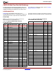
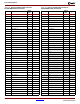
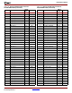
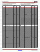
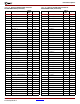
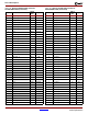
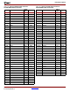
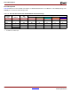
Tabl e 6 3 lists all the FG676 package pins for the
XC3SD1800A FPGA. They are sorted by bank number and
then by pin name. Pairs of pins that form a differential I/O
pair appear together in the table. The table also shows the
pin number for each pin and the pin type, as defined earlier.
Pinout Table
Note:
The grayed boxes denote a difference between the
XC3SD1800A and the XC3SD3400A devices.
Table 63:
Spartan-3A DSP FG676 Pinout for
XC3SD1800A FPGA
Bank XC3SD1800A Pin Name
FG676
Ball
Type
0 IO_L43N_0 K11 I/O
0 IO_L39N_0 K12 I/O
0 IO_L25P_0/GCLK4 K14 GCLK
0 IO_L12N_0 K16 I/O
0 IP_0 J10 INPUT
0 IO_L43P_0 J11 I/O
0 IO_L39P_0 J12 I/O
0 IP_0 J13 INPUT
0 IO_L25N_0/GCLK5 J14 GCLK
0 IP_0 J15 INPUT
0 IO_L12P_0 J16 I/O
0 IP_0/VREF_0 J17 VREF
0 IO_L47N_0 H9 I/O
0 IO_L46N_0 H10 I/O
0 IO_L35N_0 H12 I/O
0 IP_0 H13 INPUT
0 IO_L16N_0 H15 I/O
0 IO_L08P_0 H17 I/O
0 IP_0 H18 INPUT
0 IO_L52N_0/PUDC_B G8 DUAL
0 IO_L47P_0 G9 I/O
0 IO_L46P_0 G10 I/O
0 IP_0/VREF_0 G11 VREF
0 IO_L35P_0 G12 I/O
0 IO_L27N_0/GCLK9 G13 GCLK
0 IP_0 G14 INPUT
0 IO_L16P_0 G15 I/O
0 IO_L08N_0 G17 I/O
0 IO_L02P_0/VREF_0 G19 VREF
0 IO_L01P_0 G20 I/O
0 IO_L48P_0 F7 I/O
0 IO_L52P_0/VREF_0 F8 VREF
0 IO_L31N_0 F12 I/O
0IO_L27P_0/GCLK8 F13GCLK
0 IO_L24N_0 F14 I/O
0 IO_L20P_0 F15 I/O
0 IO_L13P_0 F17 I/O
0 IO_L02N_0 F19 I/O
0 IO_L01N_0 F20 I/O
0 IO_L48N_0 E7 I/O
0 IO_L37P_0 E10 I/O
0 IP_0 E11 INPUT
0 IO_L31P_0 E12 I/O
0 IO_L24P_0 E14 I/O
0 IO_L20N_0/VREF_0 E15 VREF
0 IO_L13N_0 E17 I/O
0 IP_0 E18 INPUT
0 IO_L10P_0 E21 I/O
0 IO_L44N_0 D6 I/O
0 IP_0/VREF_0 D7 VREF
0 IO_L40N_0 D8 I/O
0 IO_L37N_0 D9 I/O
0 IO_L34N_0 D10 I/O
0 IO_L32N_0/VREF_0 D11 VREF
0 IP_0 D12 INPUT
0 IO_L30P_0 D13 I/O
0 IP_0/VREF_0 D14 VREF
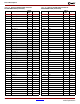
Table 63:
Spartan-3A DSP FG676 Pinout for
XC3SD1800A FPGA
(Continued)
Bank XC3SD1800A Pin Name
FG676
Ball
Type