
SpartanTM-3A DSP FPGA family Data Sheet

DC and Switching Characteristics
26 www.xilinx.com DS610-3 (v2.0) July 16, 2007
Product Specification
R
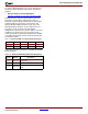
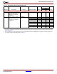
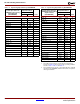
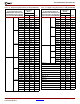
Table 21:
Input Timing Adjustments by IOSTANDARD
Convert Input Time from
LVCMOS25 to the Following
Signal Standard
(IOSTANDARD)
Add the
Adjustment Below
Units
Speed Grade
-5 -4
Single-Ended Standards
LVTTL 0.62 0.62 ns
LVCMOS33 0.54 0.54 ns
LVCMOS25 0.00 0.00 ns
LVCMOS18 0.83 0.83 ns
LVCMOS15 0.60 0.60 ns
LVCMOS12 0.31 0.31 ns
PCI33_3 0.41 0.41 ns
PCI66_3 0.41 0.41 ns
PCIX 0.41 0.41 ns
HSTL_I 0.72 0.72 ns
HSTL_III 0.77 0.77 ns
HSTL_I_18 0.69 0.69 ns
HSTL_II_18 0.69 0.69 ns
HSTL_III_18 0.79 0.79 ns
SSTL18_I 0.71 0.71 ns
SSTL18_II 0.71 0.71 ns
SSTL2_I 0.68 0.68 ns
SSTL2_II 0.68 0.68 ns
SSTL3_I 0.78 0.78 ns
SSTL3_II 0.78 0.78 ns
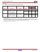
Differential Standards
LVDS_25 0.76 0.76 ns
LVDS_33 0.79 0.79 ns
BLVDS_25 0.79 0.79 ns
MINI_LVDS_25 0.78 0.78 ns
MINI_LVDS_33 0.79 0.79 ns
LVPECL_25 0.78 0.78 ns
LVPECL_33 0.79 0.79 ns
RSDS_25 0.79 0.79 ns
RSDS_33 0.77 0.77 ns
TMDS_33 0.79 0.79 ns
PPDS_25 0.79 0.79 ns
PPDS_33 0.79 0.79 ns
DIFF_HSTL_I_18 0.74 0.74 ns
DIFF_HSTL_II_18 0.72 0.72 ns
DIFF_HSTL_III_18 1.05 1.05 ns
DIFF_HSTL_I 0.72 0.72 ns
DIFF_HSTL_III 1.05 1.05 ns
DIFF_SSTL18_I 0.71 0.71 ns
DIFF_SSTL18_II 0.71 0.71 ns
DIFF_SSTL2_I 0.74 0.74 ns
DIFF_SSTL2_II 0.75 0.75 ns
DIFF_SSTL3_I 1.06 1.06 ns
DIFF_SSTL3_II 1.06 1.06 ns
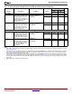
Notes:
1. The numbers in this table are tested using the methodology
presented in Ta b l e 2 5 and are based on the operating conditions
set forth in Ta bl e 7, Table 10, and Ta b l e 1 2 .
2. These adjustments are used to convert input path times originally
specified for the LVCMOS25 standard to times that correspond to
other signal standards.
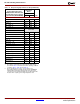
Table 21:
Input Timing Adjustments by IOSTANDARD
Convert Input Time from
LVCMOS25 to the Following
Signal Standard
(IOSTANDARD)
Add the
Adjustment Below
Units
Speed Grade
-5 -4