
SpartanTM-3A DSP FPGA family Data Sheet

DC and Switching Characteristics
DS610-3 (v2.0) July 16, 2007 www.xilinx.com 15
Product Specification
R
Single-Ended I/O Standards
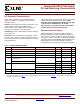
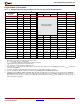
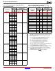
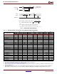
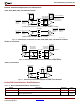
Table 10:
Recommended Operating Conditions for User I/Os Using Single-Ended Standards
IOSTANDARD
Attribute
V
CCO
for Drivers
(2)
V
REF
V
IL
V
IH
Min (V) Nom (V) Max (V) Min (V) Nom (V) Max (V) Max (V) Min (V)
LVTTL 3.0 3.3 3.6
V
REF
is not used for
these I/O standards
0.8 2.0
LVC M OS 3 3
(4)
3.0 3.3 3.6 0.8 2.0
LVC M OS 2 5
(4,5)
2.3 2.5 2.7 0.7 1.7
LVC M OS 1 8
(4)
1.65 1.8 1.95 0.38 0.8
LVC M OS 1 5
(4)
1.4 1.5 1.6 0.38 0.8
LVC M OS 1 2
(4)
1.1 1.2 1.3 0.38 0.8
PCI33_3 3.0 3.3 3.6 0.3 • V
CCO
0.5 • V
CCO
PCI66_3 3.0 3.3 3.6 0.3 • V
CCO
0.5 • V
CCO
PCIX 3.0 3.3 3.6 0.35 • V
CCO
0.5 • V
CCO
HSTL_I 1.4 1.5 1.6 0.68 0.75 0.9 V
REF
- 0.1 V
REF
+ 0.1
HSTL_III 1.4 1.5 1.6
-0.9 -V
REF
- 0.1 V
REF
+ 0.1
HSTL_I_18 1.7 1.8 1.9 0.8 0.9 1.1 V
REF
- 0.1 V
REF
+ 0.1
HSTL_II_18 1.7 1.8 1.9
-0.9 -V
REF
- 0.1 V
REF
+ 0.1
HSTL_III_18 1.7 1.8 1.9
-1.1 -V
REF
- 0.1 V
REF
+ 0.1
SSTL18_I 1.7 1.8 1.9 0.833 0.900 0.969 V
REF
- 0.125 V
REF
+ 0.125
SSTL18_II 1.7 1.8 1.9 0.833 0.900 0.969 V
REF
- 0.125 V
REF
+ 0.125
SSTL2_I 2.3 2.5 2.7 1.15 1.25 1.38 V
REF
- 0.150 V
REF
+ 0.150
SSTL2_II 2.3 2.5 2.7 1.15 1.25 1.38 V
REF
- 0.150 V
REF
+ 0.150
SSTL3_I 3.0 3.3 3.6 1.3 1.5 1.7 V
REF
- 0.2 V
REF
+ 0.2
SSTL3_II 3.0 3.3 3.6 1.3 1.5 1.7 V
REF
- 0.2 V
REF
+ 0.2
Notes:
1. Descriptions of the symbols used in this table are as follows:
V
CCO
– the supply voltage for output drivers
V
REF
– the reference voltage for setting the input switching threshold
V
IL
– the input voltage that indicates a Low logic level
V
IH
– the input voltage that indicates a High logic level
2. In general, the V
CCO
rails supply only output drivers, not input circuits. The exceptions are for LVCMOS25 inputs when V
CCAUX
= 3.3V range
and for PCI I/O standards.
3. For device operation, the maximum signal voltage (V
IH
max) can be as high as V
IN
max. See Ta bl e 3 .
4. There is approximately 100 mV of hysteresis on inputs using LVCMOS33 and LVCMOS25 I/O standards.
5. All Dedicated pins (PROG_B, DONE, SUSPEND, TCK, TDI, TDO, and TMS) draw power from the V
CCAUX
rail and use the LVCMOS25 or
LVCMOS33 standard depending on V
CCAUX
. The Dual-Purpose configuration pins use the LVCMOS25 standard before the User mode.
When using these pins as part of a standard 2.5V configuration interface, apply 2.5V to the V
CCO
lines of Banks 0, 1, and 2 at power-on as
well as throughout configuration.