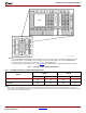
0 Spartan-3A DSP FPGA Family: Data Sheet R DS610 July 16, 2007 0 Product Specification 0 Module 1: Introduction and Ordering Information • DS610-1 (v2.0) July 16, 2007 • • • • • • • Introduction Features Architectural Overview Configuration Overview General I/O Capabilities Supported Packages and Package Marking Ordering Information Module 2: Functional Description DS610-2 (v2.0) July 16, 2007 The functionality of the Spartan™-3A DSP FPGA family is described in the following documents.
R Th is pa ge in te nt io na lly le ft bl a nk . Data Sheet 2 www.xilinx.
R < B L B Spartan-3A DSP FPGA Family: Introduction and Ordering Information DS610-1 (v2.0) July 16, 2007 Product Specification Introduction ♦ The Spartan™-3A DSP family of Field-Programmable Gate Arrays (FPGAs) solves the design challenges in most high-volume, cost-sensitive, high-performance DSP applications. The two-member family offers densities ranging from 1.8 to 3.4 million system gates, as shown in Table 1.
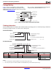
R Introduction and Ordering Information Architectural Overview The Spartan-3A DSP family architecture consists of five fundamental programmable functional elements: After applying power, the configuration data is written to the FPGA using any of seven different modes: • • Master Serial from a Xilinx Platform Flash PROM • Serial Peripheral Interface (SPI) from an industry-standard SPI serial Flash • Byte Peripheral Interface (BPI) Up from an industry-standard x8 or x8/x16 parallel NOR Flash • Sla
R Introduction and Ordering Information IOBs DCM DSP48A Slice Block RAM CLB IOBs CLBs DCM IOBs DCM Block RAM / DSP48A Slice IOBs IOBs DS610-1_01_031207 Notes: 1. The XC3SD1800A and XC3SD3400A have two DCMs on both the left and right sides, as well as the two DCMs at the top and bottom of the devices. The two DCMs on the left and right of the chips are in the middle of the outer Block RAM/DSP48A columns of the 4 or 5 columns in the selected device, as shown in the diagram above. 2.
R Introduction and Ordering Information Package Marking The “5C” and “4I” Speed Grade/Temperature Range part combinations may be dual marked as “5C/4I”. Figure 2 shows the top marking for Spartan-3A DSP FPGAs. Use the seven digits of the Lot Code to access additional information for a specific device using the Xilinx web-based Genealogy Viewer.
R Introduction and Ordering Information Revision History The following table shows the revision history for this document. Date Version 04/02/07 1.0 05/25/07 1.0.1 06/18/07 1.2 Updated for Production release. 07/16/07 2.0 Added Low-power options. DS610-1 (v2.0) July 16, 2007 Product Specification Revision Initial Xilinx release. Minor edits. www.xilinx.
R Th is pa ge in te nt io na lly le ft bl a nk . Introduction and Ordering Information 8 www.xilinx.com DS610-1 (v2.
R DS610-2 (v2.0) July 16, 2007 Spartan-3A DSP FPGA Family: Functional Description Product Specification 0 Introduction The functionality of the Spartan™-3A DSP FPGA family is described in the following documents. The topics covered in each guide are listed below.
R Th is pa g e in te nt io na lly le ft bl a nk . Functional Description 10 www.xilinx.com DS610-2 (v2.
R DS610-3 (v2.0) July 16, 2007 Spartan-3A DSP FPGA Family: DC and Switching Characteristics Product Specification 0 DC Electrical Characteristics In this section, specifications may be designated as Advance, Preliminary, or Production. These terms are defined as follows: Advance: Initial estimates are based on simulation, early characterization, and/or extrapolation from the characteristics of other families. Values are subject to change. Use as estimates, not for production.
R DC and Switching Characteristics Power Supply Specifications Table 4: Supply Voltage Thresholds for Power-On Reset Symbol Description Min Max Units VCCINTT Threshold for the VCCINT supply 0.4 1.0 V VCCAUXT Threshold for the VCCAUX supply 0.8 2.0 V VCCO2T Threshold for the VCCO Bank 2 supply 0.8 2.0 V Notes: 1. 2. VCCINT, VCCAUX, and VCCO supplies to the FPGA can be applied in any order.
R DC and Switching Characteristics General DC Characteristics for I/O Pins Table 8: General DC Characteristics of User I/O, Dual-Purpose, and Dedicated Pins Symbol Description IL Leakage current at User I/O, Input-only, Dual-Purpose, and Dedicated pins, FPGA powered IHS Test Conditions Min Typ Max Units Driver is in a high-impedance state, VIN = 0V or VCCO max, sample-tested –10 - +10 μA –10 - +10 μA Leakage current on pins during All pins except INIT_B, PROG_B, DONE, and JTAG pins hot
R DC and Switching Characteristics Quiescent Current Requirements Table 9: Quiescent Supply Current Characteristics Symbol ICCINTQ Description Quiescent VCCINT supply current Device Power Typical(2) Commercial Maximum(2) Industrial Maximum(2) Units XC3SD1800A C,I 55 390 500 mA LI 45 - 175 mA C,I 80 550 725 mA LI 70 - 300 mA C,I 0.4 4 5 mA LI 0.2 - 5 mA C,I 0.4 4 5 mA LI 0.
R DC and Switching Characteristics Single-Ended I/O Standards Table 10: Recommended Operating Conditions for User I/Os Using Single-Ended Standards IOSTANDARD Attribute VCCO for Drivers(2) VREF Min (V) Nom (V) Max (V) VIL VIH Max (V) Min (V) Min (V) Nom (V) Max (V) LVTTL 3.0 3.3 3.6 0.8 2.0 LVCMOS33(4) 3.0 3.3 3.6 0.8 2.0 LVCMOS25(4,5) 2.3 2.5 2.7 0.7 1.7 LVCMOS18(4) 1.65 1.8 1.95 0.38 0.8 0.38 0.8 VREF is not used for these I/O standards LVCMOS15(4) 1.4 1.5 1.
R DC and Switching Characteristics Table 11: DC Characteristics of User I/Os Using Single-Ended Standards (Continued) Table 11: DC Characteristics of User I/Os Using Single-Ended Standards Test Conditions IOSTANDARD Attribute LVTTL(3) LVCMOS33(3) LVCMOS25(3) LVCMOS18(3) LVCMOS15(3) LVCMOS12(3) 16 2 IOL IOH (mA) (mA) 2 –2 Test Conditions Logic Level Characteristics VOL Max (V) VOH Min (V) 0.4 2.
R DC and Switching Characteristics Differential I/O Standards VINP Internal Logic VINN VINN VID 50% VINP Differential I/O Pair Pins P N VICM GND level VICM = Input common mode voltage = VINP + VINN 2 VID = Differential input voltage = VINP - VINN DS610-3_03_061507 Figure 3: Differential Input Voltages Table 12: Recommended Operating Conditions for User I/Os Using Differential Signal Standards IOSTANDARD Attribute LVDS_25(3) VCCO for Drivers(1) Min (V) Nom (V) Max (V) 2.25 2.5 2.
R DC and Switching Characteristics VOUTP Internal Logic P N VOUTN Differential I/O Pair Pins VOH VOUTN VOD 50% VOUTP VOL VOCM GND level VOCM = Output common mode voltage = VOUTP + VOUTN 2 VOD = Output differential voltage = VOUTP - VOUTN VOH = Output voltage indicating a High logic level VOL = Output voltage indicating a Low logic level DS312-3_03_102406 Figure 4: Differential Output Voltages Table 13: DC Characteristics of User I/Os Using Differential Signal Standards IOSTANDARD Attribute
R DC and Switching Characteristics External Termination Requirements for Differential I/O LVDS, RSDS, MINI_LVDS, and PPDS I/O Standards Bank 0 and 2 Any Bank Bank 0 VCCO = 2.5V LVDS_33, MINI_LVDS_33, RSDS_33, PPDS_33 LVDS_25, MINI_LVDS_25, RSDS_25, PPDS_25 Bank 1 1/4 th of Bourns Part Number Z0 = 50Ω CAT16-PT4F4 Bank 2 VCCO = 3.
R DC and Switching Characteristics Switching Characteristics All Spartan-3A DSP FPGAs ship in two speed grades: –4 and the higher performance –5. Switching characteristics in this document are designated as Preview, Advance, Preliminary, or Production, as shown in Table 15. Each category is defined as follows: Preview: These specifications are based on estimates only and should not be used for timing analysis.
R DC and Switching Characteristics To create a Xilinx MySupport user account and sign up for automatic E-mail notification whenever this data sheet is updated: • Sign Up for Alerts on Xilinx MySupport www.xilinx.com/xlnx/xil_ans_display.jsp?getPagePath=19380 Timing parameters and their representative values are selected for inclusion below either because they are important as general design requirements or they indicate fundamental device performance characteristics.
R DC and Switching Characteristics I/O Timing Table 17: Pin-to-Pin Clock-to-Output Times for the IOB Output Path Speed Grade Symbol Description Conditions Device -5 -4 Max Max Units Clock-to-Output Times TICKOFDCM TICKOF LVCMOS25(2), 12mA output drive, Fast slew rate, with DCM(3) XC3SD1800A 3.28 3.51 ns XC3SD3400A 3.36 3.
R DC and Switching Characteristics Table 18: Pin-to-Pin Setup and Hold Times for the IOB Input Path (System Synchronous) Speed Grade Symbol Description Conditions -5 -4 Device Min Min Units Setup Times TPSDCM TPSFD When writing to the Input Flip-Flop (IFF), the time from the setup of data at the Input pin to the active transition at a Global Clock pin. The DCM is in use. No Input Delay is programmed. LVCMOS25(2), IFD_DELAY_VALUE = 0, with DCM(4) XC3SD1800A 2.65 3.11 ns XC3SD3400A 2.
R DC and Switching Characteristics Table 19: Setup and Hold Times for the IOB Input Path Speed Grade Symbol Description Conditions IFD_DELAY_ VALUE -5 -4 Device Min Min Units Setup Times TIOPICK Time from the setup of data at the Input pin to the active transition at the ICLK input of the Input Flip-Flop (IFF). No Input Delay is programmed. LVCMOS25(2) 0 All 1.36 1.
R DC and Switching Characteristics Table 20: Propagation Times for the IOB Input Path Speed Grade Symbol Description Conditions -5 -4 IFD_Delay_Value Device Max Max Units Propagation Times TIOPLI The time it takes for data to travel from the Input pin through the IFF latch to the I output with no input delay programmed LVCMOS25(2) 0 All 1.50 1.
R DC and Switching Characteristics Table 21: Input Timing Adjustments by IOSTANDARD Table 21: Input Timing Adjustments by IOSTANDARD Convert Input Time from LVCMOS25 to the Following Signal Standard (IOSTANDARD) Add the Adjustment Below Speed Grade -5 -4 Units Add the Adjustment Below Speed Grade -5 -4 Units Differential Standards Single-Ended Standards LVTTL Convert Input Time from LVCMOS25 to the Following Signal Standard (IOSTANDARD) 0.62 0.62 ns LVDS_25 0.76 0.76 ns 0.79 0.
R DC and Switching Characteristics Table 22: Timing for the IOB Output Path Speed Grade Symbol Description -5 -4 Conditions Device Max Max Units LVCMOS25(2), 12 mA output drive, Fast slew rate All 2.87 3.13 ns LVCMOS25(2), 12 mA output drive, Fast slew rate All 2.78 2.91 ns 2.70 2.85 ns 3.63 3.89 ns 8.62 9.
R DC and Switching Characteristics Table 24: Output Timing Adjustments for IOB (Continued) Table 24: Output Timing Adjustments for IOB Convert Output Time from LVCMOS25 with 12mA Drive and Fast Slew Rate to the Following Signal Standard (IOSTANDARD) Add the Adjustment Below Speed Grade -5 -4 Units Single-Ended Standards LVTTL Slow Fast QuietIO 28 Add the Adjustment Below Convert Output Time from LVCMOS25 with 12mA Drive and Fast Slew Rate to the Following Signal Standard (IOSTANDARD) Speed Gr
R DC and Switching Characteristics Table 24: Output Timing Adjustments for IOB (Continued) Add the Adjustment Below Convert Output Time from LVCMOS25 with 12mA Drive and Fast Slew Rate to the Following Signal Standard (IOSTANDARD) Speed Grade -5 -4 Units LVCMOS25 2 mA 5.33 5.33 ns 4 mA 2.81 2.81 6 mA 2.82 8 mA 1.
R DC and Switching Characteristics Table 24: Output Timing Adjustments for IOB (Continued) Convert Output Time from LVCMOS25 with 12mA Drive and Fast Slew Rate to the Following Signal Standard (IOSTANDARD) Add the Adjustment Below Speed Grade -5 -4 Units LVDS_25 1.16 1.16 ns LVDS_33 0.46 0.46 ns BLVDS_25 0.11 0.11 ns MINI_LVDS_25 0.75 0.75 ns MINI_LVDS_33 0.40 0.40 ns Differential Standards LVPECL_25 Inputs Only LVPECL_33 RSDS_25 1.42 1.42 ns RSDS_33 0.58 0.
R DC and Switching Characteristics Timing Measurement Methodology open connection, and VT is set to zero. The same measurement point (VM) that was used at the Input is also used at the Output. When measuring timing parameters at the programmable I/Os, different signal standards call for different test conditions. Table 25 lists the conditions to use for each standard.
R DC and Switching Characteristics Table 25: Test Methods for Timing Measurement at I/Os (Continued) Signal Standard (IOSTANDARD) Inputs Inputs and Outputs Outputs VREF (V) VL (V) VH (V) RT (Ω) VT (V) VM (V) SSTL3_I 1.5 VREF – 0.75 VREF + 0.75 50 1.5 VREF SSTL3_II 1.5 VREF – 0.75 VREF + 0.75 25 1.5 VREF LVDS_25 - VICM – 0.125 VICM + 0.125 50 1.2 VICM LVDS_33 - VICM – 0.125 VICM + 0.125 50 1.2 VICM BLVDS_25 - VICM – 0.125 VICM + 0.
R DC and Switching Characteristics Using IBIS Models to Simulate Load Conditions in Application IBIS models permit the most accurate prediction of timing delays for a given application. The parameters found in the IBIS model (VREF, RREF, and VMEAS) correspond directly with the parameters used in Table 25 (VT, RT, and VM). Do not confuse VREF (the termination voltage) from the IBIS model with VREF (the input-switching threshold) from the table. A fourth parameter, CREF, is always zero.
R DC and Switching Characteristics Table 27: Recommended Number of Simultaneously Switching Outputs per VCCO-GND Pair (VCCAUX=3.3V) Table 27: Recommended Number of Simultaneously Switching Outputs per VCCO-GND Pair (VCCAUX=3.
R DC and Switching Characteristics Table 27: Recommended Number of Simultaneously Switching Outputs per VCCO-GND Pair (VCCAUX=3.3V) Table 27: Recommended Number of Simultaneously Switching Outputs per VCCO-GND Pair (VCCAUX=3.
R DC and Switching Characteristics Configurable Logic Block (CLB) Timing Table 28: CLB (SLICEM) Timing Speed Grade -5 Symbol -4 Description Min Max Min Max Units When reading from the FFX (FFY) Flip-Flop, the time from the active transition at the CLK input to data appearing at the XQ (YQ) output – 0.60 – 0.68 ns TAS Time from the setup of data at the F or G input to the active transition at the CLK input of the CLB 0.18 – 0.
R DC and Switching Characteristics Table 29: CLB Distributed RAM Switching Characteristics Speed Grade -5 Symbol -4 Description Min Max Min Max Units Time from the active edge at the CLK input to data appearing on the distributed RAM output - 1.44 - 1.72 ns Clock-to-Output Times TSHCKO Setup Times TDS Setup time of data at the BX or BY input before the active transition at the CLK input of the distributed RAM -0.07 - -0.
R DC and Switching Characteristics Block RAM Timing Table 32: Block RAM Timing Speed Grade -5 Symbol Description -4 Min Max Min Max Units - 2.38 - 2.80 ns - 1.24 - 1.
R DC and Switching Characteristics DSP48A Timing To reference the DSP48A block diagram, see the XtremeDSP DSP48A for Spartan-3A DSP FPGA User Guide (UG431). Table 33: Setup Times for the DSP48A Speed Grade Symbol Description Preadder -5 -4 Multiplier Postadder Min Min Units Setup Times of Data/Control Pins to the Input Register Clock TDSPDCK_AA A input to A register CLK - - - 0.04 0.04 ns TDSPDCK_DB D input to B register CLK Yes - - 1.64 1.
R DC and Switching Characteristics Table 34: Clock to Out, Propagation Delays, and Maximum Frequency for the DSP48A Speed Grade Symbol Description -5 -4 Preadder Multiplier Postadder Max Max Units - - - 1.26 1.44 ns - Yes Yes 3.16 3.63 ns - Yes No 1.94 2.
R DC and Switching Characteristics Digital Clock Manager (DCM) Timing change with the addition of DFS or PS functions are presented in Table 35 and Table 36. For specification purposes, the DCM consists of three key components: the Delay-Locked Loop (DLL), the Digital Frequency Synthesizer (DFS), and the Phase Shifter (PS). Period jitter and cycle-cycle jitter are two of many different ways of specifying clock jitter. Both specifications describe statistical variation from a mean value.
R DC and Switching Characteristics Table 36: Switching Characteristics for the DLL Speed Grade -5 Symbol Description -4 Device Min Max Min Max Units All 5 280 5 250 MHz Output Frequency Ranges CLKOUT_FREQ_CLK0 Frequency for the CLK0 and CLK180 outputs CLKOUT_FREQ_CLK90 Frequency for the CLK90 and CLK270 outputs 5 200 5 200 MHz CLKOUT_FREQ_2X Frequency for the CLK2X and CLK2X180 outputs 10 334 10 334 MHz CLKOUT_FREQ_DV Frequency for the CLKDV output 0.3125 186 0.
R DC and Switching Characteristics Digital Frequency Synthesizer (DFS) Table 37: Recommended Operating Conditions for the DFS Speed Grade -5 Symbol Description -4 Min Max Min Max Units 0.2 333 0.
R DC and Switching Characteristics Phase Shifter (PS) Table 39: Recommended Operating Conditions for the PS in Variable Phase Mode Speed Grade -5 Symbol Description -4 Min Max Min Max Units 1 167 1 167 MHz 40% 60% 40% 60% - Operating Frequency Ranges PSCLK_FREQ (FPSCLK) Frequency for the PSCLK input Input Pulse Requirements PSCLK_PULSE PSCLK pulse width as a percentage of the PSCLK period Table 40: Switching Characteristics for the PS in Variable Phase Mode Symbol Description Phase
R DC and Switching Characteristics DNA Port Timing Table 42: DNA_PORT Interface Timing Min Max Units TDNASSU Symbol Setup time on SHIFT before the rising edge of CLK Description 1.0 – ns 0.5 – ns TDNASH Hold time on SHIFT after the rising edge of CLK TDNADSU Setup time on DIN before the rising edge of CLK 1.0 – ns TDNADH Hold time on DIN after the rising edge of CLK 0.5 – ns TDNARSU Setup time on READ before the rising edge of CLK 5.
R DC and Switching Characteristics Suspend Mode Timing Entering Suspend Mode Exiting Suspend Mode sw_gwe_cycle sw_gts_cycle SUSPEND Input tSUSPENDHIGH_AWAKE tSUSPENDLOW_AWAKE AWAKE Output tAWAKE_GWE tSUSPEND_GWE Flip-Flops, Block RAM, Distributed RAM Write Protected tAWAKE_GTS tSUSPEND_GTS FPGA Outputs Defined by SUSPEND constraint tSUSPEND_DISABLE FPGA Inputs, Interconnect tSUSPEND_ENABLE Blocked DS610-3_08_061207 Figure 9: Suspend Mode Timing Table 43: Suspend Mode Timing Parameters Symbol
R DC and Switching Characteristics Configuration and JTAG Timing General Configuration Power-On/Reconfigure Timing 1.2V VCCINT (Supply) 1.0V VCCAUX (Supply) 2.0V VCCO Bank 2 (Supply) 1.0V 2.5V or 3.3V TPOR PROG_B (Input) TPROG INIT_B (Open-Drain) TPL TICCK CCLK (Output) DS529-3_01_112906 Notes: 1. 2. 3. The VCCINT, VCCAUX, and VCCO supplies can be applied in any order. The Low-going pulse on PROG_B is optional after power-on but necessary for reconfiguration without a power cycle.
R DC and Switching Characteristics Configuration Clock (CCLK) Characteristics Table 45: Master Mode CCLK Output Period by ConfigRate Option Setting Symbol TCCLK1 Description CCLK clock period by ConfigRate setting ConfigRate Setting Temperature Range Minimum 1 (power-on value) Commercial 1,254 TCCLK3 3 TCCLK6 6 TCCLK7 7 TCCLK8 8 TCCLK10 10 TCCLK12 12 TCCLK13 13 TCCLK17 17 TCCLK22 22 TCCLK25 25 TCCLK27 27 TCCLK33 33 TCCLK44 44 TCCLK50 50 TCCLK100 100 Industrial 1,180
R DC and Switching Characteristics Table 46: Master Mode CCLK Output Frequency by ConfigRate Option Setting Description ConfigRate Setting Temperature Range Equivalent CCLK clock frequency by ConfigRate setting 1 (power-on value) Commercial Symbol FCCLK1 FCCLK3 3 FCCLK6 6 FCCLK7 7 FCCLK8 8 FCCLK10 10 FCCLK12 12 FCCLK13 13 FCCLK17 17 FCCLK22 22 FCCLK25 25 FCCLK27 27 FCCLK33 33 FCCLK44 44 FCCLK50 50 FCCLK100 100 Minimum 0.400 Industrial Commercial 1.
R DC and Switching Characteristics Master Serial and Slave Serial Mode Timing PROG_B (Input) INIT_B (Open-Drain) TMCCH TSCCH TMCCL TSCCL CCLK (Input/Output) TDCC DIN (Input) 1/FCCSER TCCD Bit 0 Bit 1 Bit n Bit n+1 TCCO DOUT (Output) Bit n-64 Bit n-63 DS312-3_05_103105 Figure 11: Waveforms for Master Serial and Slave Serial Configuration Table 49: Timing for the Master Serial and Slave Serial Configuration Modes Description Slave/ Master The time from the falling transition on the CCLK pin t
R DC and Switching Characteristics Slave Parallel Mode Timing PROG_B (Input) INIT_B (Open-Drain) TSMCSCC TSMCCCS CSI_B (Input) TSMCCW TSMWCC RDWR_B (Input) TMCCH TSCCH TMCCL TSCCL CCLK (Input) TSMDCC D0 - D7 (Inputs) TSMCCD Byte 0 1/FCCPAR Byte 1 Byte n Byte n+1 DS529-3_02_051607 Notes: 1. It is possible to abort configuration by pulling CSI_B Low in a given CCLK cycle, then switching RDWR_B Low or High in any subsequent cycle for which CSI_B remains Low.
R DC and Switching Characteristics Serial Peripheral Interface (SPI) Configuration Timing PROG_B (Input) PUDC_B PUDC_B must be stable before INIT_B goes High and constant throughout the configuration process. (Input) VS[2:0] <1:1:1> (Input) M[2:0] Mode input pins M[2:0] and variant select input pins VS[2:0] are sampled when INIT_B goes High. After this point, input values do not matter until DONE goes High, at which point these pins become user-I/O pins.
R DC and Switching Characteristics Table 52: Configuration Timing Requirements for Attached SPI Serial Flash Symbol Description Requirement Units TCCS SPI serial Flash PROM chip-select time T CCS ≤ T MCCL 1 – T CCO ns TDSU SPI serial Flash PROM data input setup time T DSU ≤ T MCCL 1 – T CCO ns TDH SPI serial Flash PROM data input hold time TV SPI serial Flash PROM data clock-to-output time fC or fR Maximum SPI serial Flash PROM clock frequency (also depends on specific read command used)
R DC and Switching Characteristics Byte Peripheral Interface (BPI) Configuration Timing PROG_B (Input) PUDC_B (Input) PUDC_B must be stable before INIT_B goes High and constant throughout the configuration process. M[2:0] (Input) Mode input pins M[2:0] are sampled when INIT_B goes High. After this point, input values do not matter until DONE goes High, at which point the mode pins become user-I/O pins.
R DC and Switching Characteristics Table 54: Configuration Timing Requirements for Attached Parallel NOR Flash Symbol Description Requirement Units TCE (tELQV) Parallel NOR Flash PROM chip-select time T CE ≤ T INITADDR ns TOE (tGLQV) Parallel NOR Flash PROM output-enable time T OE ≤ T INITADDR ns TACC (tAVQV) Parallel NOR Flash PROM read access time T ACC ≤ T CCLKn ( min ) – T CCO – T DCC – PCB ns TBYTE (tFLQV, tFHQV) For x8/x16 PROMs only: BYTE# to output valid time(3) T BYTE ≤ T INITAD
R DC and Switching Characteristics IEEE 1149.1/1553 JTAG Test Access Port Timing TCCH TCCL TCK (Input) 1/FTCK TTCKTMS TTMSTCK TMS (Input) TTDITCK TTCKTDI TDI (Input) TTCKTDO TDO (Output) DS099_06_040703 Figure 15: JTAG Waveforms Table 55: Timing for the JTAG Test Access Port All Speed Grades Symbol Description Min Max Units 1.0 11.0 ns All functions except those shown below 7.0 – ns Boundary scan commands (INTEST, EXTEST, SAMPLE) 13.0 7.
R DC and Switching Characteristics Revision History The following table shows the revision history for this document. Date Version 04/02/07 1.0 05/25/07 1.0.1 06/18/07 1.2 Updated for v1.29 production speed files. Noted banking rules in Table 11 and Table 12. Added DIFF_HSTL_I and DIFF_HSTL_III to Table 12, Table 13, and Table 25. Updated TMDS DC characteristics in Table 13. Updated I/O Test Method values in Table 25. Added Simultaneously Switching Output limits in Table 27.
R Th is pa ge in te nt io na lly le ft bl a nk . DC and Switching Characteristics 58 www.xilinx.com DS610-3 (v2.
R DS610-4 (v2.0) July 16, 2007 Spartan-3A DSP FPGA Family: Pinout Descriptions Product Specification 0 Introduction This section describes how the various pins on a Spartan™-3A DSP FPGA connect within the supported component packages and provides device-specific thermal characteristics. For general information on the pin functions and the package characteristics, see the Packaging section in: • UG331: Spartan-3 Generation FPGA User Guide http://www.xilinx.com/bvdocs/userguides/ug331.
R Pinout Descriptions Table 56: Types of Pins on Spartan-3A DSP FPGAs (Continued) Type/Color Code Description GND Dedicated ground pin. The number of GND pins depends on the package used. All must be connected. GND VCCAUX Dedicated auxiliary power supply pin. The number of VCCAUX pins depends on the package used. All must be connected. VCCAUX VCCINT Dedicated internal core logic power supply pin. The number of VCCINT pins depends on the package used. All must be connected to +1.2V.
R Pinout Descriptions Package Thermal Characteristics The power dissipated by an FPGA application has implications on package selection and system design. The power consumed by a Spartan-3A DSP FPGA is reported using either the XPower Power Estimator or the XPower Analyzer calculator integrated in the Xilinx ISE™ development software. Table 59 provides the thermal characteristics for the various Spartan-3A DSP device package offerings.
R Pinout Descriptions CS484: 484-Ball Chip-Scale Ball Grid Array The 484-ball chip-scale ball grid array, CS484, supports both the XC3SD1800A and XC3SD3400A FPGAs. There are no pinout differences between the two devices. Table 60 lists all the CS484 package pins. They are sorted by bank number and then by pin name. Pairs of pins that form a differential I/O pair appear together in the table. The table also shows the pin number for each pin and the pin type, as defined earlier.
R Pinout Descriptions Table 60: Spartan-3A DSP CS484 Pinout (Continued) Bank Pin Name CS484 Ball Type Table 60: Spartan-3A DSP CS484 Pinout (Continued) Bank Pin Name CS484 Ball Type 0 IO_L17N_0/GCLK5 F11 GCLK 1 IO_L29P_1/A16 K16 DUAL 0 IP_0 F12 INPUT 1 IP_L23N_1 K17 INPUT 0 IO_L13N_0 F13 I/O 1 IO_L24N_1 K18 I/O 0 IO_L13P_0 F14 I/O 1 IO_L24P_1 K19 I/O 0 IO_L05N_0 F15 I/O 1 IO_L25P_1/A12 K20 DUAL 0 IO_L04N_0 F16 I/O 1 IO_L22N_1/A11 K22 DUAL 0 IO_L23P_
R Pinout Descriptions Table 60: Spartan-3A DSP CS484 Pinout (Continued) Bank 64 Pin Name CS484 Ball Type Table 60: Spartan-3A DSP CS484 Pinout (Continued) Bank CS484 Ball Pin Name Type 1 IO_L03N_1/A1 V20 DUAL 2 IO_L27P_2 AB19 I/O 1 IP_L08P_1 V22 INPUT 2 IO_L30N_2 AB20 I/O 1 IO_L03P_1/A0 W19 DUAL 2 IO_L02N_2/CSO_B U7 DUAL 1 IP_L04N_1/VREF_1 W20 VREF 2 IO_L11N_2 U8 I/O 1 IP_L04P_1 W21 INPUT 2 IO_L10N_2 U9 I/O 1 IO_L06P_1 W22 I/O 2 IO_L14N_2/D4 U10 DUAL
R Pinout Descriptions Table 60: Spartan-3A DSP CS484 Pinout (Continued) Bank Pin Name CS484 Ball Type Table 60: Spartan-3A DSP CS484 Pinout (Continued) Bank Pin Name CS484 Ball Type 2 IP_2/VREF_2 Y14 VREF 3 IO_L17P_3 K2 I/O 2 IO_L24N_2/D3 Y15 DUAL 3 IO_L17N_3 K3 I/O 2 IO_L29N_2 Y16 I/O 3 IO_L13P_3 K4 I/O 2 IO_L29P_2 Y17 I/O 3 IO_L13N_3 K5 I/O 2 IO_L26P_2/D2 Y18 DUAL 3 IO_L15P_3 K6 I/O 2 IO_L26N_2/D1 Y19 DUAL 3 IO_L19N_3/IRDY2/LHCLK3 L1 LHCLK 2 VCCO_
R Pinout Descriptions Table 60: Spartan-3A DSP CS484 Pinout (Continued) Bank 66 Pin Name CS484 Ball Type Table 60: Spartan-3A DSP CS484 Pinout (Continued) Bank Pin Name CS484 Ball Type 3 IO_L36P_3 V4 I/O GND GND H19 GND 3 IO_L35N_3 W1 I/O GND GND J9 GND 3 IO_L37N_3 W2 I/O GND GND J11 GND 3 IO_L37P_3 W3 I/O GND GND J13 GND 3 IO_L35P_3 Y1 I/O GND GND J15 GND 3 IP_L39P_3 Y2 INPUT GND GND K8 GND 3 VCCO_3 E2 VCCO GND GND K10 GND 3 VCCO_3 J2 VC
R Pinout Descriptions Table 60: Spartan-3A DSP CS484 Pinout (Continued) Bank Pin Name CS484 Ball Type Table 60: Spartan-3A DSP CS484 Pinout (Continued) Bank Pin Name CS484 Ball Type GND GND T14 GND VCCINT VCCINT G7 VCCINT GND GND T15 GND VCCINT VCCINT G16 VCCINT GND GND T19 GND VCCINT VCCINT H9 VCCINT GND GND T21 GND VCCINT VCCINT H11 VCCINT GND GND U6 GND VCCINT VCCINT H13 VCCINT GND GND U11 GND VCCINT VCCINT H15 VCCINT GND GND U17 GND VCCINT V
R Pinout Descriptions User I/Os by Bank Table 61 and Table 62 indicates how the user-I/O pins are distributed between the four I/O banks on the CS484 package. The AWAKE pin is counted as a Dual-Purpose I/O.
R Pinout Descriptions CS484 Footprint Bank 0 1 Left Half of Package (top view) I/O: Unrestricted, 156 general-purpose user I/O. 41 A GND PROG_ B B TMS VCCAUX C INPUT: Unrestricted, general-purpose input pin. 2 D I/O I/O L02N_3 L02P_3 INPUT L04P_3 TDI INPUT E 52 DUAL: Configuration, AWAKE pins, then possible user I/O. 28 VREF: User I/O or input voltage reference for bank. 32 CLK: User I/O, input, or clock buffer input. F G H 4 GND: Ground.
R Pinout Descriptions Bank 0 12 INPUT GND 13 14 I/O I/O L11P_0 L10P_0 I/O L11N_0 I/O I/O L14N_0 L14P_0 VCCAUX I/O L17P_0 GCLK4 VCCO_0 15 INPUT I/O L10N_0 I/O INPUT L12N_0 VREF_0 I/O I/O I/O L09N_0 L12P_0 L08P_0 I/O L09P_0 VCCO_0 16 I/O L06P_0 VREF_0 GND 17 I/O L06N_0 I/O L03P_0 18 INPUT VCCO_0 I/O 19 20 I/O I/O L07N_0 0 I/O I/O L02N_0 L07P_0 I/O I/O L08N_0 L03N_0 L02P_0 VREF_0 GND INPUT INPUT INPUT VCCAUX I/O I/O I/O GND L38N_1 A25 L38P_1 A24 L3
R Pinout Descriptions FG676: 676-Ball Fine-Pitch Ball Grid Array The 676-ball fine-pitch ball grid array, FG676, supports both the XC3SD1800A and the XC3SD3400A FPGAs. There are multiple pinout differences between the two devices. For a list of differences and migration advice, see the "Footprint Migration Differences" section. XC3SD1800A FPGA Table 63 lists all the FG676 package pins for the XC3SD1800A FPGA. They are sorted by bank number and then by pin name.
R Pinout Descriptions Table 63: Spartan-3A DSP FG676 Pinout for XC3SD1800A FPGA (Continued) Bank 72 XC3SD1800A Pin Name Table 63: Spartan-3A DSP FG676 Pinout for XC3SD1800A FPGA (Continued) FG676 Ball Type Bank XC3SD1800A Pin Name FG676 Ball Type 0 IO_L22P_0 D16 I/O 0 IO_L07P_0 B23 I/O 0 IO_L21P_0 D17 I/O 0 IO_L51P_0 A3 I/O 0 IO_L17P_0 D18 I/O 0 IO_L45P_0 A4 I/O 0 IO_L11P_0 D20 I/O 0 IP_0 A7 INPUT 0 IO_L10N_0 D21 I/O 0 IO_L38P_0 A8 I/O 0 IO_L05P_0 D22 I
R Pinout Descriptions Table 63: Spartan-3A DSP FG676 Pinout for XC3SD1800A FPGA (Continued) Bank XC3SD1800A Pin Name Table 63: Spartan-3A DSP FG676 Pinout for XC3SD1800A FPGA (Continued) FG676 Ball Type Bank XC3SD1800A Pin Name FG676 Ball Type 0 VCCO_0 B16 VCCO 1 IO_L25N_1/A3 R22 DUAL 0 VCCO_0 B22 VCCO 1 IP_L28P_1/VREF_1 R23 VREF 1 IO_L01P_1/HDC Y20 DUAL 1 IP_L28N_1 R24 INPUT 1 IO_L01N_1/LDC2 Y21 DUAL 1 IO_L29P_1/A8 R25 DUAL 1 IO_L13P_1 Y22 I/O 1 IO_L29N_1/A9
R Pinout Descriptions Table 63: Spartan-3A DSP FG676 Pinout for XC3SD1800A FPGA (Continued) Bank 74 XC3SD1800A Pin Name Table 63: Spartan-3A DSP FG676 Pinout for XC3SD1800A FPGA (Continued) FG676 Ball Type Bank XC3SD1800A Pin Name FG676 Ball Type 1 IO_L50N_1 K21 I/O 1 IO_L03N_1/A1 AC24 DUAL 1 IO_L46N_1 K22 I/O 1 IO_L05N_1 AC25 I/O 1 IO_L46P_1 K23 I/O 1 IO_L06P_1 AC26 I/O 1 IP_L40P_1 K24 INPUT 1 IO_L07P_1 AB23 I/O 1 IO_L41P_1 K25 I/O 1 IO_L07N_1/VREF_1 AB24
R Pinout Descriptions Table 63: Spartan-3A DSP FG676 Pinout for XC3SD1800A FPGA (Continued) Bank XC3SD1800A Pin Name Table 63: Spartan-3A DSP FG676 Pinout for XC3SD1800A FPGA (Continued) FG676 Ball Type Bank XC3SD1800A Pin Name FG676 Ball Type 2 IO_L46P_2 W17 I/O 2 IO_L26N_2/GCLK15 AE13 GCLK 2 IO_L09P_2 V10 I/O 2 IO_L28N_2/GCLK3 AE14 GCLK 2 IO_L13P_2 V11 I/O 2 IO_L32N_2/DOUT AE15 DUAL 2 IO_L16P_2 V12 I/O 2 IO_L33P_2 AE17 I/O 2 IO_L20P_2 V13 I/O 2 IO_L36N_2/D1
R Pinout Descriptions Table 63: Spartan-3A DSP FG676 Pinout for XC3SD1800A FPGA (Continued) Bank 76 XC3SD1800A Pin Name Table 63: Spartan-3A DSP FG676 Pinout for XC3SD1800A FPGA (Continued) FG676 Ball Type Bank XC3SD1800A Pin Name FG676 Ball Type 2 IO_L41N_2 AC20 I/O 2 VCCO_2 AE5 VCCO 2 IO_L45N_2 AC21 I/O 2 VCCO_2 AE11 VCCO 2 IO_2 AC22 I/O 2 VCCO_2 AE16 VCCO 2 IP_2/VREF_2 AB6 VREF 2 VCCO_2 AE22 VCCO 2 IO_L14N_2 AB7 I/O 2 VCCO_2 AB8 VCCO 2 IO_L15P_2 AB9
R Pinout Descriptions Table 63: Spartan-3A DSP FG676 Pinout for XC3SD1800A FPGA (Continued) Bank XC3SD1800A Pin Name Table 63: Spartan-3A DSP FG676 Pinout for XC3SD1800A FPGA (Continued) FG676 Ball Type Bank XC3SD1800A Pin Name FG676 Ball Type 3 IO_L48P_3 T10 I/O 3 IO_L18N_3 L7 I/O 3 IO_L36P_3/VREF_3 R1 VREF 3 IO_L15N_3 L9 I/O 3 IO_L36N_3 R2 I/O 3 IO_L15P_3 L10 I/O 3 IO_L37P_3 R3 I/O 3 IP_L24N_3 K1 INPUT 3 IO_L37N_3 R4 I/O 3 IO_L23N_3 K2 I/O 3 IO_L40P_3 R
R Pinout Descriptions Table 63: Spartan-3A DSP FG676 Pinout for XC3SD1800A FPGA (Continued) Bank 78 XC3SD1800A Pin Name Table 63: Spartan-3A DSP FG676 Pinout for XC3SD1800A FPGA (Continued) FG676 Ball Type Bank XC3SD1800A Pin Name FG676 Ball Type 3 IP_L04P_3 C2 INPUT GND GND T1 GND 3 IO_L02N_3 B1 I/O GND GND T6 GND 3 IO_L02P_3 B2 I/O GND GND T12 GND 3 IP_L66P_3 AE1 INPUT GND GND T14 GND 3 IP_L66N_3/VREF_3 AE2 VREF GND GND T16 GND 3 IO_L65P_3 AD1 I/O GN
R Pinout Descriptions Table 63: Spartan-3A DSP FG676 Pinout for XC3SD1800A FPGA (Continued) Bank XC3SD1800A Pin Name Table 63: Spartan-3A DSP FG676 Pinout for XC3SD1800A FPGA (Continued) FG676 Ball Type Bank XC3SD1800A Pin Name FG676 Ball Type GND GND F21 GND VCCAUX VCCAUX P17 VCCAUX GND GND F26 GND VCCAUX VCCAUX N10 VCCAUX GND GND C3 GND VCCAUX VCCAUX L5 VCCAUX GND GND C9 GND VCCAUX VCCAUX K13 VCCAUX GND GND C14 GND VCCAUX VCCAUX J18 VCCAUX GND GND C19
R Pinout Descriptions User I/Os by Bank Table 64 indicates how the available user-I/O pins are distributed between the four I/O banks on the FG676 package. The AWAKE pin is counted as a Dual-Purpose I/O.
R Pinout Descriptions FG676 Footprint XC3SD1800A FPGA Bank 0 Left Half of Package (top view) A B I/O: Unrestricted, 314 general-purpose user I/O. C INPUT: Unrestricted, 82 general-purpose input pin. E F DUAL: Configuration, 52 AWAKE pins, then possible user I/O. G VREF: User I/O or input 39 voltage reference for bank. H J CLK: User I/O, input, or 32 clock buffer input.
R Pinout Descriptions Bank 0 I/O L26N_0 GCLK7 I/O L26P_0 GCLK6 GND INPUT VREF_0 I/O L24P_0 15 I/O L23N_0 I/O L23P_0 INPUT VCCO_0 19 20 I/O I/O I/O L18N_0 L15N_0 L14N_0 I/O I/O I/O L19N_0 L18P_0 L15P_0 I/O I/O I/O L21N_0 L19P_0 L17N_0 INPUT ∇ I/O I/O L16P_0 I/O L16N_0 I/O INPUT I/O GND INPUT I/O I/O I/O L22P_0 L21P_0 L17P_0 ∇ INPUT VCCO_0 I/O L20N_0 VREF_0 L20P_0 L25N_0 GCLK5 GND 18 I/O I/O GND 17 L22N_0 L24N_0 INPUT 16 VCCAUX GND INPUT ∇ VCCO_0
R Pinout Descriptions XC3SD3400A FPGA Table 65 lists all the FG676 package pins for the XC3SD3400A FPGA. They are sorted by bank number and then by pin name. Pairs of pins that form a differential I/O pair appear together in the table. Table 65 also shows the pin number for each pin and the pin type, as defined earlier. An electronic version of this package pinout table and footprint diagram is available for download from the Xilinx website at: http://www.xilinx.com/bvdocs/publications/s3adsp_pin.
R Pinout Descriptions Table 65: Spartan-3A DSP FG676 Pinout for XC3SD3400A FPGA (Continued) Bank 84 XC3SD3400A Pin Name FG676 Ball Table 65: Spartan-3A DSP FG676 Pinout for XC3SD3400A FPGA (Continued) Type Bank XC3SD3400A Pin Name FG676 Ball Type 0 IO_L05P_0 D22 I/O 0 IO_L33P_0 A10 I/O 0 IO_L06P_0 D23 I/O 0 IO_L29P_0 A12 I/O 0 IO_L44P_0 C5 I/O 0 IP_0 A13 INPUT 0 IO_L41N_0 C6 I/O 0 IO_L26N_0/GCLK7 A14 GCLK 0 IO_L42N_0 C7 I/O 0 IO_L23N_0 A15 I/O 0 IO_L40P_0
R Pinout Descriptions Table 65: Spartan-3A DSP FG676 Pinout for XC3SD3400A FPGA (Continued) Bank XC3SD3400A Pin Name FG676 Ball Table 65: Spartan-3A DSP FG676 Pinout for XC3SD3400A FPGA (Continued) Type Bank XC3SD3400A Pin Name FG676 Ball Type 1 IO_L12N_1 U18 I/O 1 IO_L47N_1 M18 I/O 1 IO_L12P_1 U19 I/O 1 IO_L47P_1 M19 I/O 1 IO_L10N_1 U20 I/O 1 IO_L42N_1/A17 M20 DUAL 1 IO_L14P_1 U21 I/O 1 IO_L45P_1 M21 I/O 1 IO_L21N_1 U22 I/O 1 IO_L45N_1 M22 I/O 1 IO_L23P_1
R Pinout Descriptions Table 65: Spartan-3A DSP FG676 Pinout for XC3SD3400A FPGA (Continued) Bank 86 XC3SD3400A Pin Name FG676 Ball Table 65: Spartan-3A DSP FG676 Pinout for XC3SD3400A FPGA (Continued) Type Bank XC3SD3400A Pin Name FG676 Ball Type 1 IP_1/VREF_1 G25 VREF 2 IO_L12P_2 Y10 I/O 1 IO_L58P_1/VREF_1 F22 VREF 2 IO_L17P_2/RDWR_B Y12 DUAL 1 IO_L56N_1 F23 I/O 2 IO_L25N_2/GCLK13 Y13 GCLK 1 IO_L54N_1 F24 I/O 2 IO_L27P_2/GCLK0 Y14 GCLK 1 IO_L54P_1 F25 I/O 2 I
R Pinout Descriptions Table 65: Spartan-3A DSP FG676 Pinout for XC3SD3400A FPGA (Continued) Bank XC3SD3400A Pin Name FG676 Ball Table 65: Spartan-3A DSP FG676 Pinout for XC3SD3400A FPGA (Continued) Type Bank XC3SD3400A Pin Name FG676 Ball Type 2 IO_L48P_2 AF23 I/O 2 IO_L14P_2 AC8 I/O 2 IO_L52P_2/D0/DIN/MISO AF24 DUAL 2 IO_L15N_2 AC9 I/O 2 IO_L51P_2 AF25 I/O 2 IP_2/VREF_2 AC10 VREF 2 IO_L06P_2 AE3 I/O 2 IO_L23N_2 AC11 I/O 2 IO_L07P_2 AE4 I/O 2 IO_L21N_2 AC12 I
R Pinout Descriptions Table 65: Spartan-3A DSP FG676 Pinout for XC3SD3400A FPGA (Continued) Bank 88 XC3SD3400A Pin Name FG676 Ball Table 65: Spartan-3A DSP FG676 Pinout for XC3SD3400A FPGA (Continued) Type Bank XC3SD3400A Pin Name FG676 Ball Type 2 VCCO_2 AB8 VCCO 3 IO_L37N_3 R4 I/O 2 VCCO_2 AB14 VCCO 3 IO_L40P_3 R5 I/O 2 VCCO_2 AB19 VCCO 3 IO_L40N_3 R6 I/O 3 IO_L53P_3 Y1 I/O 3 IO_L45N_3 R7 I/O 3 IO_L53N_3 Y2 I/O 3 IO_L45P_3 R8 I/O 3 IP_3 Y3 INPUT 3 IO
R Pinout Descriptions Table 65: Spartan-3A DSP FG676 Pinout for XC3SD3400A FPGA (Continued) Bank XC3SD3400A Pin Name FG676 Ball Table 65: Spartan-3A DSP FG676 Pinout for XC3SD3400A FPGA (Continued) Type Bank XC3SD3400A Pin Name FG676 Ball Type 3 IO_L23N_3 K2 I/O 3 IO_L65P_3 AD1 I/O 3 IO_L23P_3 K3 I/O 3 IO_L65N_3 AD2 I/O 3 IO_L22N_3 K4 I/O 3 IO_L60N_3 AC1 I/O 3 IO_L22P_3 K5 I/O 3 IO_L64P_3 AC2 I/O 3 IO_L18P_3 K6 I/O 3 IO_L64N_3 AC3 I/O 3 IO_L13P_3 K7 I/O
R Pinout Descriptions Table 65: Spartan-3A DSP FG676 Pinout for XC3SD3400A FPGA (Continued) Bank 90 XC3SD3400A Pin Name FG676 Ball Table 65: Spartan-3A DSP FG676 Pinout for XC3SD3400A FPGA (Continued) Type Bank XC3SD3400A Pin Name FG676 Ball Type GND GND P12 GND GND GND C9 GND GND GND P16 GND GND GND C14 GND GND GND P19 GND GND GND C19 GND GND GND P24 GND GND GND C24 GND GND GND N3 GND GND GND B24 GND GND GND N8 GND GND GND B25 GND GND GND N11 GN
R Pinout Descriptions Table 65: Spartan-3A DSP FG676 Pinout for XC3SD3400A FPGA (Continued) Bank XC3SD3400A Pin Name FG676 Ball Table 65: Spartan-3A DSP FG676 Pinout for XC3SD3400A FPGA (Continued) Type Bank XC3SD3400A Pin Name FG676 Ball Type GND GND A23 GND VCCINT VCCINT T11 VCCINT GND GND A26 GND VCCINT VCCINT T13 VCCINT AB21 CONFIG VCCINT VCCINT T15 VCCINT VCCAUX DONE VCCAUX PROG_B A2 CONFIG VCCINT VCCINT R12 VCCINT VCCAUX TDI G7 JTAG VCCINT VCCINT R14 VC
R Pinout Descriptions User I/Os by Bank Table 66 indicates how the available user-I/O pins are distributed between the four I/O banks on the FG676 package. The AWAKE pin is counted as a Dual-Purpose I/O.
R Pinout Descriptions FG676 Footprint XC3SD3400A FPGA Bank 0 A Left Half of Package (top view) B 1 2 3 4 5 I/O I/O GND GND PROG_ B L51P_0 L45P_0 I/O I/O I/O I/O L02N_3 L02P_3 L51N_0 L45N_0 INPUT C I/O: Unrestricted, 314 general-purpose user I/O. D INPUT: Unrestricted, 34 general-purpose input pin. E F DUAL: Configuration, 52 AWAKE pins, then possible user I/O. G H J CLK: User I/O, input, or 32 clock buffer input. CONFIG: Dedicated configuration pins, SUSPEND pin.
R Pinout Descriptions Bank 0 I/O L26N_0 GCLK7 I/O L26P_0 GCLK6 GND INPUT VREF_0 I/O L24P_0 15 I/O L23N_0 I/O L23P_0 INPUT VCCO_0 19 20 I/O I/O I/O L18N_0 L15N_0 L14N_0 I/O I/O I/O L19N_0 L18P_0 L15P_0 I/O I/O I/O L21N_0 L19P_0 L17N_0 GND ∇ I/O I/O L16P_0 I/O L16N_0 I/O INPUT I/O GND GND I/O I/O I/O L22P_0 L21P_0 L17P_0 ∇ INPUT VCCO_0 I/O L20N_0 VREF_0 L20P_0 L25N_0 GCLK5 GND 18 I/O I/O GND 17 L22N_0 L24N_0 INPUT 16 VCCAUX GND GND ∇ VCCO_0 I/O L
R Pinout Descriptions Footprint Migration Differences There are multiple migration footprint differences between the XC3SD1800A and the XC3SD3400A in the FG676 package. These migration footprint differences are shown in Table 67. Migration from the XC3S1400A Spartan-3A device in the FG676 package to a Spartan-3A DSP device in the FG676 package is also possible. The XC3S1800A pin migration differences have been added to Table 67 for designs migrating between these devices.
R Pinout Descriptions Table 67: FG676 Footprint Migration Differences (Continued) Spartan-3A Spartan-3A DSP Spartan-3A DSP FG676 Ball XC3S1400A Type XC3S1400A Bank XC3SD1800A Type XC3SD1800A Bank XC3SD3400A Type XC3SD3400A Bank FG676 Ball Y8 N.C. N.C. IP_2 2 VCCINT VCCINT Y8 Y11 IP_2 2 IP_2 2 VCCINT VCCINT Y11 Y18 N.C. N.C. IP_2 2 VCCINT VCCINT Y18 Y19 N.C. N.C. IP_2/VREF_2 2 VCCINT VCCINT Y19 W18 N.C. N.C.
R Pinout Descriptions Revision History The following table shows the revision history for this document. Date Version Revision 04/02/07 1.0 Initial Xilinx release. 05/25/07 1.1 Updates to Table 58, Table 60, Table 61, Table 62, Table 63, Table 64, Table 65, Table 66. Corrected VREF pins in XC3S1800A FG676 (Table 67). Updated FG676 package footprints for XC3SD1800A FPGA (Figure 17) and XC3SD3400A FPGA (Figure 18). Minor edits. 06/18/07 1.2 Updated for Production release. 07/16/07 2.
R Th is pa ge in te nt io na lly le ft bl a nk . Pinout Descriptions 98 www.xilinx.com DS610-4 (v2.