
User's Manual
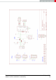
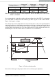
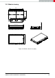

19.4 Footprint
18,0
24,0
1,0
2,0 4,0
2,0
22,0 1,5
4,0
2,2
6,0
Figure 20: Footprint and dimensions [mm]
The following points have to be considered:
• To avoid the risk of short circuits, a minimum clearance of at least 14 mm between the
opposing pad rows has to be maintained! No routing on the top layer of a carrier PCB
(i.e. "under" the module) shall be performed.
• For the module variant with integrated antenna the marked corner area of 7.3 x 13.8 m-
m has to be kept free from metal, on any layer.
• The four bottom side pads are optionally for the firmware update using JTAG can be
left open when JTAG update is not needed in the customer’s application.
• This footprint is also compatible to the radio modules Tarvos-I, Tarvos-II, Thadeus and
Titania.
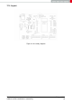
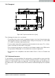
19.5 Antenna free area
To avoid influence and mismatching of the antenna the recommended free area around the
antenna should be maintained. As rule of thumb a minimum distance of metal parts to the
antenna of λ/10 should be kept (see figure
20
). Even though metal parts would influence
the characteristic of the antenna, but the direct influence and matching keep an acceptable
level.
Themisto-I reference manual version 1.0 © August 2019
www.we-online.com/wireless-connectivity 97