
User's Manual


ATM100
Version 1.0 page 3 of 14
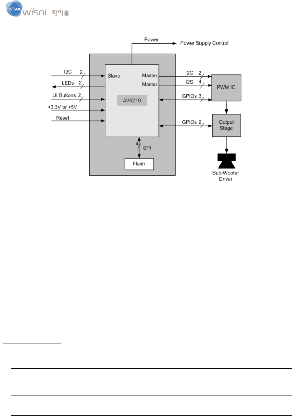
Typical Sub-Woofer Implement
A simple low cost implementation of a sub-woofer product design is shown in Figure 2. The sub amplifier consists of a
PWM chip plus an output stage device, but no external MCU is required as the ATM100 RX module performs the control
function using the I2C master communication port in conjunction with multiple GPIOs. +5V power and
an optional reset signal are supplied to the ATM100 RX module and I2C slave communication can be used to control the
module if required. Several GPIOs can be used to drive LEDs, or to connect to UI buttons. Typically 2 LEDs may be used
and 1 button for pairing purposes. Another button could be used, for example, to implement a “bass enhance” feature.
Another GPIO can be used to control the main power supply for the unit. The ATM100 RX module will remain always
powered up but a GPIO control line is used to enable/disable the higher voltage rail for the amplifier output circuitry. If the
wireless link is lost (when the sound bar, or ATM100 TX module is powered down) the ATM100 RX module can, after a
timeout period, power down the amplifier section to conserve power and to help meet energy start requirements.
The I2C master port from the ATM100 RX module can communicate, control, and initialize external audio ICs such as the
PWM chip in this example.
Other GPIOs can be used to detect fault conditions (over temperature etc) and notify the module. The audio is routed from
the ATM100 RX module to the amplifier circuit with the I2S output port which can be configured as either a master or a
slave as required. MCLK can also be generated from the SWA RX module as a ~12.288MHz clock if required.
I/O interfaces description
I/O interfaces Description
+5.0V supply The ATM100 module is configured to accept a nominal +5.0V supply.
Reset Active low reset input. This pin is driven from an open collector/drain device such that it can be
pulled to ground for the active reset state but, when released, must go to a high impedance state.
This pin should not be actively driven high, as the AV5100 internal reset circuit will not operate
correctly.
I2S In Port The I2S input port can be configured as a master or slave. Consequently BCLK and LRCK can
be either inputs or outputs. In addition, MCLK can be sourced by the module. Since the AV5100
IC contains a sample rate converter, MCLK is not required to be supplied to the module when it