
User's Manual


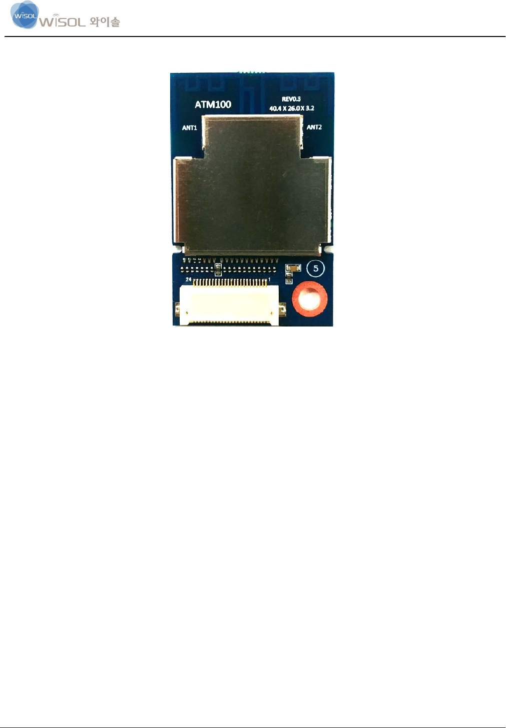
ATM100
Version 1.0 page 2 of 14
3. General Function
The ATM100 module is available in 2 variations; digital input transmitter module or digital output receiver module. There
is a separate I2S port for digital audio input and output functions and either of these can be configured to be a master or a
slave – only the input or output port can be active at any time. In addition, MCLK can be generated from the module, or
input to the module as required by the system application.
The highly integrated nature of the AV6210 transceiver IC results in few external components being required for the
ATM100 module design. 2 PCB antennas are used to achieve increased range, and to offer diversity, and the simple RF
path consists only of the antennas, associated tuning components, the RF switch and a LC balun connected to the AV6210
IC. A 16MHz crystal generates the AV6210 system clock signal used as the basis for all RF and digital audio signals. In
addition, a 2Mb flash memory stores the factory based firmware, as well as firmware upgrade images and configuration
parameters. The module firmware enables upgrades to be performed by the I2C slave interface or over-the-air. The module
can be controlled from an external host device via the I2C interface. The I2C master port allows the module to control
other system audio devices such as a sub-woofer amplifier system without having to add another MCU to the product
design. Up to a maximum of 17 GPIOs are supported with the ATM100 module including I2C and I2S signals. This large
number of GPIOs can be leveraged to Implement low cost sub-woofer designs as outlined below.
The ATM100 module offers a standard and low latency firmware with different over the air sample rate. While the
standard 22.2KSps over the air sample rate optimizes audio quality and WiFi coexistence performance; Lower audio
latency can be achieved by using the low-latency 44.4KSps over the air sample rate.