
Data Sheet


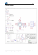


Table Of Contents
- WT32C3-S1 User manual V1.0.0-加警告语 5.25
- 警告语
- Federal Communication Commission Statement (FCC, U.S.)
- FCC Caution:
- IMPORTANT NOTES
- Co-location warning:
- OEM integration instructions:
- Validity of using the module certification:
- End product labeling:
- Information that must be placed in the end user manual:
- Integration instructions for host product manufactures according to KDB 996369 D03 OEM Manual v01

V1.0.0
Copyright ©2020 Wireless-Tag Technology Co., Ltd. All Rights Reserved. http://www.wireless-tag.com 12
5.4 Peripheral Schematic
This is the typical application circuit of the module connected with peripheral components (for example,
power supply, antenna, reset button, JTAG interface, and UART interface).
Figure 7 Application Circuit
Soldering the EPAD to the ground of the base board is not a must, though doing so can get
optimized thermal performance. If you do want to solder it, please ensure that you apply the correct
amount of soldering paste.
To ensure the power supply to the ESP32-C3 family chip is stable during power-up, it is advised
to add an RC delay circuit at the EN pin. The recommended setting for the RC delay circuit is usually
R = 10 kΩ and C = 1 µF. However, specific parameters should be adjusted based on the power-up
timing of the module and the power-up and reset sequence timing of the chip.