
Data Sheet


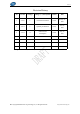


Table Of Contents

V1.0.2
Copyright ©2020 Wireless-Tag Technology Co., Ltd. All Rights Reserved. http://www.wireless-tag.com 5
watchdog reset, crystal clock glitch detection reset), the latches of the strapping pins sample the voltage
level as strapping bits of “0” or “1”, and hold these bits until the chip is powered down or shut down.
By default, GPIO9 is connected to the internal pull-up resistor. If GPIO9 is not connected or connected to
an external high-impedance circuit, the latched bit value will be “1”.
To change the strapping bit values, you can apply the external pull-down/pull-up resistances, or use the
host MCU’s GPIOs to control the voltage level of these pins when powering on ESP32-C3 family.
After reset, the strapping pins work as normal-function pins.
Refer to Table 2 for a detailed boot-mode configuration of the strapping pins.
Note:
Some pins have been internally pulled up, please refer to the schematic diagram.
Table 2 Strapping Pins
Figure 3 shows the setup and hold times for the strapping pin before and after the CHIP_EN signal goes
high.
Figure 3 Setup and Hold Times for the Strapping Pin
Booting Mode
1
Pin
Default
SPI Boot
Download Boot
GPIO2
N/A
1
1
GPIO8
N/A
Don't care
1
GPIO9
Internal
pull-up
1
0
Enabling/Disabling ROM Code Print During Booting
Pin
Default
Functionality
GPIO8
N/A
When the value of eFuse field UART_PRINT_CONTROL is
0, print is enabled and not controlled by GPIO8.
1, if GPIO8 is 0, print is enabled; if GPIO8 is 1, it is disabled.
2, if GPIO8 is 0, print is disabled; if GPIO8 is 1, it is enabled.
3, print is disabled and not controlled by GPIO8.
Parameter Descriptions of Setup and Hold Times for the Strapping Pin
Parameter
Description
Min
t0
Setup time before CHIP_EN goes from low to high
0ms
t1
Hold time after CHIP_EN goes high
3ms