
User's Manual
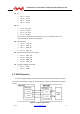
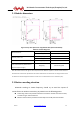
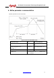
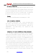
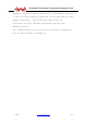
Table Of Contents

Wi-linktech Communication Technologies (Shanghai) Co.,Ltd.
To maximize RF performance, the user motherboard layout should follow the following
recommendations:
1) Antenna clearance area: the user mainboard located directly below the module
antenna area shall not have any copper foil wiring (including power supply,
ground and signal layer).
2) Module position: the module should ideally be placed in the corner of the user's
main board, and the PCB antenna is located at the far end of the main board. This
position minimizes the clearance area of the antenna.
(Refer to the definition of antenna clearance area below)
Figure 5-3 Antenna Keep out
5.3 Object diagram of module
Figure 5-4 WLT
8258 module
2019.03
www
.w
i
-
li
nk
te
ch
.c
om
14