
Datasheet


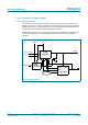

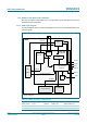
Table Of Contents
- 1. General description
- 2. Features and benefits
- 3. Applications
- 4. Quick reference data
- 5. Ordering information
- 6. Block diagram
- 7. Pinning information
- 8. Functional description
- 8.1 80C51
- 8.2 General purpose IOs configurations
- 8.3 Host interfaces
- 8.4 Power management
- 8.5 Power clock and reset controller
- 8.6 Contactless Interface Unit (CIU)
- 8.6.1 Feature list
- 8.6.2 Simplified block diagram
- 8.6.3 Reader/Writer modes
- 8.6.4 ISO/IEC 18092, ECMA 340 NFCIP-1 operating mode
- 8.6.5 Card operating modes
- 8.6.6 Overall CIU block diagram
- 8.6.7 Transmitter control
- 8.6.8 RF level detector
- 8.6.9 Antenna presence self test
- 8.6.10 Random generator
- 8.6.11 Data mode detector
- 8.6.12 Serial data switch
- 8.6.13 NFC-WI/S2C interface support
- 8.6.14 Hardware support for FeliCa and NFC polling
- 8.6.15 CRC co-processor
- 8.6.16 FIFO buffer
- 8.6.17 CIU_timer
- 8.6.18 Interrupt request system
- 8.6.19 CIU Power Reduction Modes
- 8.6.20 CIU command set
- 8.6.20.1 General description
- 8.6.20.2 General behavior
- 8.6.20.3 Commands overview
- 8.6.20.4 Idle command
- 8.6.20.5 Config command
- 8.6.20.6 Generate RandomID command
- 8.6.20.7 CalcCRC command
- 8.6.20.8 Transmit command
- 8.6.20.9 NoCmdChange command
- 8.6.20.10 Receive command
- 8.6.20.11 Transceive command
- 8.6.20.12 AutoColl command
- 8.6.20.13 MFAuthent command
- 8.6.20.14 SoftReset command
- 8.6.21 CIU tests signals
- 8.6.22 CIU memory map
- 8.6.23 CIU register description
- 8.6.23.1 CIU register bit behavior
- 8.6.23.2 CIU_SIC_CLK_en register (6330h)
- 8.6.23.3 CIU_Command register (D1h or 6331h)
- 8.6.23.4 CIU_CommIEn register (D2h or 6332h)
- 8.6.23.5 CIU_DivIEn register (D3h or 6333h)
- 8.6.23.6 CIU_CommIrq register (D4h or 6334h)
- 8.6.23.7 CIU_DivIrq register (D5h or 6335h)
- 8.6.23.8 CIU_Error register (D6h or 6336h)
- 8.6.23.9 CIU_Status1 register (DFh or 6337h)
- 8.6.23.10 CIU_Status2 register (E9h or 6338h)
- 8.6.23.11 CIU_FIFOData register (EAh or 6339h)
- 8.6.23.12 CIU_FIFOLevel register (EBh or 633Ah)
- 8.6.23.13 CIU_WaterLevel register (ECh or 633Bh)
- 8.6.23.14 CIU_Control register (EDh or 633Ch)
- 8.6.23.15 CIU_BitFraming register (EEh or 633Dh)
- 8.6.23.16 CIU_Coll register (EFh or 633Eh)
- 8.6.23.17 CIU_Mode register (6301h)
- 8.6.23.18 CIU_TxMode register (6302h)
- 8.6.23.19 CIU_RxMode register (6303h)
- 8.6.23.20 CIU_TxControl register (6304h)
- 8.6.23.21 CIU_TxAuto register (6305h)
- 8.6.23.22 CIU_TxSel register (6306h)
- 8.6.23.23 CIU_RxSel register (6307h)
- 8.6.23.24 CIU_RxThreshold register (6308h)
- 8.6.23.25 CIU_Demod register (6309h)
- 8.6.23.26 CIU_FelNFC1 register (630Ah)
- 8.6.23.27 CIU_FelNFC2 register (630Bh)
- 8.6.23.28 CIU_MifNFC register (630Ch)
- 8.6.23.29 CIU_ManualRCV register (630Dh)
- 8.6.23.30 CIU_TypeB register (630Eh)
- 8.6.23.31 CIU_CRCResultMSB register (6311h)
- 8.6.23.32 CIU_CRCResultLSB register (6312h)
- 8.6.23.33 CIU_GsNOff register (6313h)
- 8.6.23.34 CIU_ModWidth register (6314h)
- 8.6.23.35 CIU_TxBitPhase register (6315h)
- 8.6.23.36 CIU_RFCfg register (6316h)
- 8.6.23.37 CIU_GsNOn register (6317h)
- 8.6.23.38 CIU_CWGsP register (6318h)
- 8.6.23.39 CIU_ModGsP register (6319h)
- 8.6.23.40 CIU_TMode register (631Ah)
- 8.6.23.41 CIU_TPrescaler register (631Bh)
- 8.6.23.42 CIU_TReload_hi register (631Ch)
- 8.6.23.43 CIU_TReloadVal_lo register (631Dh)
- 8.6.23.44 CIU_TCounterVal_hi register (631Eh)
- 8.6.23.45 Register CIU_TCounterVal_lo (631Fh)
- 8.6.23.46 CIU_TestSel1 register (6321h)
- 8.6.23.47 CIU_TestSel2 register (6322h)
- 8.6.23.48 CIU_TestPinEn register (6323h)
- 8.6.23.49 CIU_TestPinValue register (6324h)
- 8.6.23.50 CIU_TestBus register (6325h)
- 8.6.23.51 CIU_AutoTest register (6326h)
- 8.6.23.52 CIU_Version register (6327h)
- 8.6.23.53 CIU_AnalogTest register (6328h)
- 8.6.23.54 CIU_TestDAC1 register (6329h)
- 8.6.23.55 CIU_TestDAC2 register (632Ah)
- 8.6.23.56 CIU_TestADC register (632Bh)
- 8.6.23.57 CIU_RFlevelDet register (632Fh)
- 8.7 Registers map
- 9. Limiting values
- 10. Recommended operating conditions
- 11. Thermal characteristics
- 12. Characteristics
- 12.1 Power management characteristics
- 12.2 Overcurrent detection
- 12.3 Current consumption characteristics
- 12.4 Antenna presence self test thresholds
- 12.5 Typical 27.12 MHz Crystal requirements
- 12.6 Pin characteristics for 27.12 MHz XTAL Oscillator (OSCIN, OSCOUT)
- 12.7 RSTPD_N input pin characteristics
- 12.8 Input pin characteristics for I0 and I1
- 12.9 RSTOUT_N output pin characteristics
- 12.10 Input/output characteristics for pin P70_IRQ
- 12.11 Input/output pin characteristics for P30 / UART_RX, P31 / UART_TX, P32_INT0, P33_INT1
- 12.12 Input/output pin characteristics for P34 / SIC_CLK
- 12.13 Input/output pin characteristics for P35
- 12.14 Input pin characteristics for NSS / P50_SCL / HSU_RX
- 12.15 Input/output pin characteristics for MOSI / SDA / HSU_TX
- 12.16 Input/output pin characteristics for MISO / P71 and SCK / P72
- 12.17 Input pin characteristics for SIGIN
- 12.18 Output pin characteristics for SIGOUT
- 12.19 Output pin characteristics for LOADMOD
- 12.20 Input pin characteristics for RX
- 12.21 Output pin characteristics for AUX1/AUX2
- 12.22 Output pin characteristics for TX1/TX2
- 12.23 Timing for Reset and Hard-Power-Down
- 12.24 Timing for the SPI compatible interface
- 12.25 Timing for the I2C interface
- 13. Application information
- 14. Package outline
- 15. Abbreviations
- 16. Revision history
- 17. Legal information
- 18. Contact information
- 19. Contents

PN532_C1 All information provided in this document is subject to legal disclaimers. © NXP B.V. 2017. All rights reserved.
Product data sheet
COMPANY PUBLIC
Rev. 3.6 — 28 November 2017
115436 84 of 222
NXP Semiconductors
PN532/C1
Near Field Communication (NFC) controller
8.4 Power management
Figure 19 “Power management scheme” depicts the internal and external power
distribution management. Power is supplied to the PN532 via pins VBAT and PVDD.
VBAT is driven by the battery and is used to supply the all blocks excluding the host
interface. PVDD is connected to the host’s power supply and powers the PN532’s host
interface. No specific sequencing is required between the two supply rails: VBAT can be
present without PVDD and vice versa.
An internal low drop-out (LDO) voltage regulator generates DVDD and SVDD, which are
used to supply the internal digital logic and the secure IC respectively. DVDD is also
routed externally to supply AVDD (analog power) and TVDD (transmit power). DVDD,
AVDD and TVDD must be separately decoupled.
When another host interface than SPI is used, the PN532 can be used with reduced
functionalities; all functionalities, except those related to the PVDD supplied pins (like host
interfaces) when:
PVDD < 0.4V
5.5V > VBAT > 2.7V
3.6V > RSTPD_N > VBAT * 0.65
Fig 19. Power management scheme
4.7
F
100nF
DVDD
AVDD
TVDD
PN532
VBAT
Low DropOut
PVDD
HOST
VDD
VDDHOST (1.6V -> 3.6V)
VBAT PN532 (2.7V -> 5.5V)
Secure
SVDD
4.7
F
100nF
100nF
IC
SVDD switch
regulator
LDO
Power distribution
RSTPD_N
internal DVDD