
Datasheet
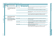


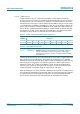


Table Of Contents
- 1. General description
- 2. Features and benefits
- 3. Applications
- 4. Quick reference data
- 5. Ordering information
- 6. Block diagram
- 7. Pinning information
- 8. Functional description
- 8.1 80C51
- 8.2 General purpose IOs configurations
- 8.3 Host interfaces
- 8.4 Power management
- 8.5 Power clock and reset controller
- 8.6 Contactless Interface Unit (CIU)
- 8.6.1 Feature list
- 8.6.2 Simplified block diagram
- 8.6.3 Reader/Writer modes
- 8.6.4 ISO/IEC 18092, ECMA 340 NFCIP-1 operating mode
- 8.6.5 Card operating modes
- 8.6.6 Overall CIU block diagram
- 8.6.7 Transmitter control
- 8.6.8 RF level detector
- 8.6.9 Antenna presence self test
- 8.6.10 Random generator
- 8.6.11 Data mode detector
- 8.6.12 Serial data switch
- 8.6.13 NFC-WI/S2C interface support
- 8.6.14 Hardware support for FeliCa and NFC polling
- 8.6.15 CRC co-processor
- 8.6.16 FIFO buffer
- 8.6.17 CIU_timer
- 8.6.18 Interrupt request system
- 8.6.19 CIU Power Reduction Modes
- 8.6.20 CIU command set
- 8.6.20.1 General description
- 8.6.20.2 General behavior
- 8.6.20.3 Commands overview
- 8.6.20.4 Idle command
- 8.6.20.5 Config command
- 8.6.20.6 Generate RandomID command
- 8.6.20.7 CalcCRC command
- 8.6.20.8 Transmit command
- 8.6.20.9 NoCmdChange command
- 8.6.20.10 Receive command
- 8.6.20.11 Transceive command
- 8.6.20.12 AutoColl command
- 8.6.20.13 MFAuthent command
- 8.6.20.14 SoftReset command
- 8.6.21 CIU tests signals
- 8.6.22 CIU memory map
- 8.6.23 CIU register description
- 8.6.23.1 CIU register bit behavior
- 8.6.23.2 CIU_SIC_CLK_en register (6330h)
- 8.6.23.3 CIU_Command register (D1h or 6331h)
- 8.6.23.4 CIU_CommIEn register (D2h or 6332h)
- 8.6.23.5 CIU_DivIEn register (D3h or 6333h)
- 8.6.23.6 CIU_CommIrq register (D4h or 6334h)
- 8.6.23.7 CIU_DivIrq register (D5h or 6335h)
- 8.6.23.8 CIU_Error register (D6h or 6336h)
- 8.6.23.9 CIU_Status1 register (DFh or 6337h)
- 8.6.23.10 CIU_Status2 register (E9h or 6338h)
- 8.6.23.11 CIU_FIFOData register (EAh or 6339h)
- 8.6.23.12 CIU_FIFOLevel register (EBh or 633Ah)
- 8.6.23.13 CIU_WaterLevel register (ECh or 633Bh)
- 8.6.23.14 CIU_Control register (EDh or 633Ch)
- 8.6.23.15 CIU_BitFraming register (EEh or 633Dh)
- 8.6.23.16 CIU_Coll register (EFh or 633Eh)
- 8.6.23.17 CIU_Mode register (6301h)
- 8.6.23.18 CIU_TxMode register (6302h)
- 8.6.23.19 CIU_RxMode register (6303h)
- 8.6.23.20 CIU_TxControl register (6304h)
- 8.6.23.21 CIU_TxAuto register (6305h)
- 8.6.23.22 CIU_TxSel register (6306h)
- 8.6.23.23 CIU_RxSel register (6307h)
- 8.6.23.24 CIU_RxThreshold register (6308h)
- 8.6.23.25 CIU_Demod register (6309h)
- 8.6.23.26 CIU_FelNFC1 register (630Ah)
- 8.6.23.27 CIU_FelNFC2 register (630Bh)
- 8.6.23.28 CIU_MifNFC register (630Ch)
- 8.6.23.29 CIU_ManualRCV register (630Dh)
- 8.6.23.30 CIU_TypeB register (630Eh)
- 8.6.23.31 CIU_CRCResultMSB register (6311h)
- 8.6.23.32 CIU_CRCResultLSB register (6312h)
- 8.6.23.33 CIU_GsNOff register (6313h)
- 8.6.23.34 CIU_ModWidth register (6314h)
- 8.6.23.35 CIU_TxBitPhase register (6315h)
- 8.6.23.36 CIU_RFCfg register (6316h)
- 8.6.23.37 CIU_GsNOn register (6317h)
- 8.6.23.38 CIU_CWGsP register (6318h)
- 8.6.23.39 CIU_ModGsP register (6319h)
- 8.6.23.40 CIU_TMode register (631Ah)
- 8.6.23.41 CIU_TPrescaler register (631Bh)
- 8.6.23.42 CIU_TReload_hi register (631Ch)
- 8.6.23.43 CIU_TReloadVal_lo register (631Dh)
- 8.6.23.44 CIU_TCounterVal_hi register (631Eh)
- 8.6.23.45 Register CIU_TCounterVal_lo (631Fh)
- 8.6.23.46 CIU_TestSel1 register (6321h)
- 8.6.23.47 CIU_TestSel2 register (6322h)
- 8.6.23.48 CIU_TestPinEn register (6323h)
- 8.6.23.49 CIU_TestPinValue register (6324h)
- 8.6.23.50 CIU_TestBus register (6325h)
- 8.6.23.51 CIU_AutoTest register (6326h)
- 8.6.23.52 CIU_Version register (6327h)
- 8.6.23.53 CIU_AnalogTest register (6328h)
- 8.6.23.54 CIU_TestDAC1 register (6329h)
- 8.6.23.55 CIU_TestDAC2 register (632Ah)
- 8.6.23.56 CIU_TestADC register (632Bh)
- 8.6.23.57 CIU_RFlevelDet register (632Fh)
- 8.7 Registers map
- 9. Limiting values
- 10. Recommended operating conditions
- 11. Thermal characteristics
- 12. Characteristics
- 12.1 Power management characteristics
- 12.2 Overcurrent detection
- 12.3 Current consumption characteristics
- 12.4 Antenna presence self test thresholds
- 12.5 Typical 27.12 MHz Crystal requirements
- 12.6 Pin characteristics for 27.12 MHz XTAL Oscillator (OSCIN, OSCOUT)
- 12.7 RSTPD_N input pin characteristics
- 12.8 Input pin characteristics for I0 and I1
- 12.9 RSTOUT_N output pin characteristics
- 12.10 Input/output characteristics for pin P70_IRQ
- 12.11 Input/output pin characteristics for P30 / UART_RX, P31 / UART_TX, P32_INT0, P33_INT1
- 12.12 Input/output pin characteristics for P34 / SIC_CLK
- 12.13 Input/output pin characteristics for P35
- 12.14 Input pin characteristics for NSS / P50_SCL / HSU_RX
- 12.15 Input/output pin characteristics for MOSI / SDA / HSU_TX
- 12.16 Input/output pin characteristics for MISO / P71 and SCK / P72
- 12.17 Input pin characteristics for SIGIN
- 12.18 Output pin characteristics for SIGOUT
- 12.19 Output pin characteristics for LOADMOD
- 12.20 Input pin characteristics for RX
- 12.21 Output pin characteristics for AUX1/AUX2
- 12.22 Output pin characteristics for TX1/TX2
- 12.23 Timing for Reset and Hard-Power-Down
- 12.24 Timing for the SPI compatible interface
- 12.25 Timing for the I2C interface
- 13. Application information
- 14. Package outline
- 15. Abbreviations
- 16. Revision history
- 17. Legal information
- 18. Contact information
- 19. Contents

PN532_C1 All information provided in this document is subject to legal disclaimers. © NXP B.V. 2017. All rights reserved.
Product data sheet
COMPANY PUBLIC
Rev. 3.6 — 28 November 2017
115436 64 of 222
NXP Semiconductors
PN532/C1
Near Field Communication (NFC) controller
8.3.2.9 I
2
CDAT register
I
2
CDAT contains a byte of I
2
C data to be transmitted or a byte which has just been
received. The CPU can read from and write to this 8-bit SFR while it is not in the process
of shifting a byte. This occurs when the I
2
C interface is in a defined state and the serial
interrupt flag SI is set to logic 1. Data in I
2
CDAT remains stable as long as SI is set to logic
1. The first bit to be transmitted is the MSB (bit 7), and, after a byte has been received, the
first bit of received data is located at the MSB of I
2
CDAT. While data is being shifted out,
data on the bus is simultaneously being shifted in; I
2
CDAT always contains the last data
byte present on the bus. Thus, in the event of lost arbitration, the transition from Master
Transmitter to Slave Receiver is made with the correct data in I
2
CDAT.
I
2
CDAT[7:0] and the ACK flag form a 9-bit shift register which shifts in or shifts out an 8-bit
byte, followed by an acknowledge bit. The ACK flag is controlled by the I
2
C interface
hardware and cannot be accessed by the CPU. I
2
C data are shifted through the ACK flag
into I
2
CDAT on the rising edges of clock pulses on P50_SCL. When a byte has been
shifted into I
2
CDAT, the I
2
C data are available in I
2
CDAT, and the acknowledge bit is
returned by the control logic during the ninth clock pulse. I
2
C data are shifted out from
I
2
CDAT via a buffer on the falling edges of clock pulses on P50_SCL.
When the CPU writes to I
2
CDAT, the buffer is loaded with the contents of I
2
CDAT[7] which
is the first bit to be transmitted to the SDA line. After nine serial clock pulses, the eight bits
in I
2
CDAT will have been transmitted to the SDA line, and the acknowledge bit will be
present in ACK. Note that the eight transmitted bits are shifted back into I
2
CDAT.
Table 85. I
2
CDAT register (SFR: address DAh) bit allocation
Bit 7 6 5 4 3 2 1 0
Symbol I
2
CDAT[7:0]
Reset 00000000
Access R/W R/W R/W R/W R/W R/W R/W R/W
Table 86. Description of I
2
CDAT bits
Bit Symbol Description
7 to 0 I
2
CDAT[7:0] I2C data. Eight bits to be transmitted or just received. A logic 1 in
I
2
CDAT corresponds to a logic 1 on the I
2
C bus, and a logic 0
corresponds to a logic 0 on the bus. I
2
C data shift through I
2
CDAT
from right to left.