
Datasheet
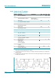
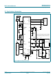
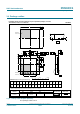

Table Of Contents
- 1. General description
- 2. Features and benefits
- 3. Applications
- 4. Quick reference data
- 5. Ordering information
- 6. Block diagram
- 7. Pinning information
- 8. Functional description
- 8.1 80C51
- 8.2 General purpose IOs configurations
- 8.3 Host interfaces
- 8.4 Power management
- 8.5 Power clock and reset controller
- 8.6 Contactless Interface Unit (CIU)
- 8.6.1 Feature list
- 8.6.2 Simplified block diagram
- 8.6.3 Reader/Writer modes
- 8.6.4 ISO/IEC 18092, ECMA 340 NFCIP-1 operating mode
- 8.6.5 Card operating modes
- 8.6.6 Overall CIU block diagram
- 8.6.7 Transmitter control
- 8.6.8 RF level detector
- 8.6.9 Antenna presence self test
- 8.6.10 Random generator
- 8.6.11 Data mode detector
- 8.6.12 Serial data switch
- 8.6.13 NFC-WI/S2C interface support
- 8.6.14 Hardware support for FeliCa and NFC polling
- 8.6.15 CRC co-processor
- 8.6.16 FIFO buffer
- 8.6.17 CIU_timer
- 8.6.18 Interrupt request system
- 8.6.19 CIU Power Reduction Modes
- 8.6.20 CIU command set
- 8.6.20.1 General description
- 8.6.20.2 General behavior
- 8.6.20.3 Commands overview
- 8.6.20.4 Idle command
- 8.6.20.5 Config command
- 8.6.20.6 Generate RandomID command
- 8.6.20.7 CalcCRC command
- 8.6.20.8 Transmit command
- 8.6.20.9 NoCmdChange command
- 8.6.20.10 Receive command
- 8.6.20.11 Transceive command
- 8.6.20.12 AutoColl command
- 8.6.20.13 MFAuthent command
- 8.6.20.14 SoftReset command
- 8.6.21 CIU tests signals
- 8.6.22 CIU memory map
- 8.6.23 CIU register description
- 8.6.23.1 CIU register bit behavior
- 8.6.23.2 CIU_SIC_CLK_en register (6330h)
- 8.6.23.3 CIU_Command register (D1h or 6331h)
- 8.6.23.4 CIU_CommIEn register (D2h or 6332h)
- 8.6.23.5 CIU_DivIEn register (D3h or 6333h)
- 8.6.23.6 CIU_CommIrq register (D4h or 6334h)
- 8.6.23.7 CIU_DivIrq register (D5h or 6335h)
- 8.6.23.8 CIU_Error register (D6h or 6336h)
- 8.6.23.9 CIU_Status1 register (DFh or 6337h)
- 8.6.23.10 CIU_Status2 register (E9h or 6338h)
- 8.6.23.11 CIU_FIFOData register (EAh or 6339h)
- 8.6.23.12 CIU_FIFOLevel register (EBh or 633Ah)
- 8.6.23.13 CIU_WaterLevel register (ECh or 633Bh)
- 8.6.23.14 CIU_Control register (EDh or 633Ch)
- 8.6.23.15 CIU_BitFraming register (EEh or 633Dh)
- 8.6.23.16 CIU_Coll register (EFh or 633Eh)
- 8.6.23.17 CIU_Mode register (6301h)
- 8.6.23.18 CIU_TxMode register (6302h)
- 8.6.23.19 CIU_RxMode register (6303h)
- 8.6.23.20 CIU_TxControl register (6304h)
- 8.6.23.21 CIU_TxAuto register (6305h)
- 8.6.23.22 CIU_TxSel register (6306h)
- 8.6.23.23 CIU_RxSel register (6307h)
- 8.6.23.24 CIU_RxThreshold register (6308h)
- 8.6.23.25 CIU_Demod register (6309h)
- 8.6.23.26 CIU_FelNFC1 register (630Ah)
- 8.6.23.27 CIU_FelNFC2 register (630Bh)
- 8.6.23.28 CIU_MifNFC register (630Ch)
- 8.6.23.29 CIU_ManualRCV register (630Dh)
- 8.6.23.30 CIU_TypeB register (630Eh)
- 8.6.23.31 CIU_CRCResultMSB register (6311h)
- 8.6.23.32 CIU_CRCResultLSB register (6312h)
- 8.6.23.33 CIU_GsNOff register (6313h)
- 8.6.23.34 CIU_ModWidth register (6314h)
- 8.6.23.35 CIU_TxBitPhase register (6315h)
- 8.6.23.36 CIU_RFCfg register (6316h)
- 8.6.23.37 CIU_GsNOn register (6317h)
- 8.6.23.38 CIU_CWGsP register (6318h)
- 8.6.23.39 CIU_ModGsP register (6319h)
- 8.6.23.40 CIU_TMode register (631Ah)
- 8.6.23.41 CIU_TPrescaler register (631Bh)
- 8.6.23.42 CIU_TReload_hi register (631Ch)
- 8.6.23.43 CIU_TReloadVal_lo register (631Dh)
- 8.6.23.44 CIU_TCounterVal_hi register (631Eh)
- 8.6.23.45 Register CIU_TCounterVal_lo (631Fh)
- 8.6.23.46 CIU_TestSel1 register (6321h)
- 8.6.23.47 CIU_TestSel2 register (6322h)
- 8.6.23.48 CIU_TestPinEn register (6323h)
- 8.6.23.49 CIU_TestPinValue register (6324h)
- 8.6.23.50 CIU_TestBus register (6325h)
- 8.6.23.51 CIU_AutoTest register (6326h)
- 8.6.23.52 CIU_Version register (6327h)
- 8.6.23.53 CIU_AnalogTest register (6328h)
- 8.6.23.54 CIU_TestDAC1 register (6329h)
- 8.6.23.55 CIU_TestDAC2 register (632Ah)
- 8.6.23.56 CIU_TestADC register (632Bh)
- 8.6.23.57 CIU_RFlevelDet register (632Fh)
- 8.7 Registers map
- 9. Limiting values
- 10. Recommended operating conditions
- 11. Thermal characteristics
- 12. Characteristics
- 12.1 Power management characteristics
- 12.2 Overcurrent detection
- 12.3 Current consumption characteristics
- 12.4 Antenna presence self test thresholds
- 12.5 Typical 27.12 MHz Crystal requirements
- 12.6 Pin characteristics for 27.12 MHz XTAL Oscillator (OSCIN, OSCOUT)
- 12.7 RSTPD_N input pin characteristics
- 12.8 Input pin characteristics for I0 and I1
- 12.9 RSTOUT_N output pin characteristics
- 12.10 Input/output characteristics for pin P70_IRQ
- 12.11 Input/output pin characteristics for P30 / UART_RX, P31 / UART_TX, P32_INT0, P33_INT1
- 12.12 Input/output pin characteristics for P34 / SIC_CLK
- 12.13 Input/output pin characteristics for P35
- 12.14 Input pin characteristics for NSS / P50_SCL / HSU_RX
- 12.15 Input/output pin characteristics for MOSI / SDA / HSU_TX
- 12.16 Input/output pin characteristics for MISO / P71 and SCK / P72
- 12.17 Input pin characteristics for SIGIN
- 12.18 Output pin characteristics for SIGOUT
- 12.19 Output pin characteristics for LOADMOD
- 12.20 Input pin characteristics for RX
- 12.21 Output pin characteristics for AUX1/AUX2
- 12.22 Output pin characteristics for TX1/TX2
- 12.23 Timing for Reset and Hard-Power-Down
- 12.24 Timing for the SPI compatible interface
- 12.25 Timing for the I2C interface
- 13. Application information
- 14. Package outline
- 15. Abbreviations
- 16. Revision history
- 17. Legal information
- 18. Contact information
- 19. Contents

PN532_C1 All information provided in this document is subject to legal disclaimers. © NXP B.V. 2017. All rights reserved.
Product data sheet
COMPANY PUBLIC
Rev. 3.6 — 28 November 2017
115436 219 of 222
continued >>
NXP Semiconductors
PN532/C1
Near Field Communication (NFC) controller
19. Contents
1 General description. . . . . . . . . . . . . . . . . . . . . . 1
2 Features and benefits . . . . . . . . . . . . . . . . . . . . 3
3 Applications . . . . . . . . . . . . . . . . . . . . . . . . . . . . 4
4 Quick reference data . . . . . . . . . . . . . . . . . . . . . 4
5 Ordering information. . . . . . . . . . . . . . . . . . . . . 5
6 Block diagram . . . . . . . . . . . . . . . . . . . . . . . . . . 6
7 Pinning information. . . . . . . . . . . . . . . . . . . . . . 7
7.1 Pinning . . . . . . . . . . . . . . . . . . . . . . . . . . . . . . . 7
7.2 Pin description . . . . . . . . . . . . . . . . . . . . . . . . . 8
8 Functional description . . . . . . . . . . . . . . . . . . 10
8.1 80C51 . . . . . . . . . . . . . . . . . . . . . . . . . . . . . . 10
8.1.1 PN532 memory map. . . . . . . . . . . . . . . . . . . . 11
8.1.2 Data memory . . . . . . . . . . . . . . . . . . . . . . . . . 12
8.1.2.1 IDATA memory . . . . . . . . . . . . . . . . . . . . . . . . 12
8.1.2.2 XRAM memory . . . . . . . . . . . . . . . . . . . . . . . . 14
8.1.3 Program memory . . . . . . . . . . . . . . . . . . . . . . 15
8.1.4 PCON module . . . . . . . . . . . . . . . . . . . . . . . . 16
8.1.5 Interrupt Controller . . . . . . . . . . . . . . . . . . . . . 16
8.1.5.1 Interrupt vectors . . . . . . . . . . . . . . . . . . . . . . . 16
8.1.5.2 Interrupt enable: IE0 and IE1 registers. . . . . . 17
8.1.5.3 Interrupt prioritization: IP0 and IP1 registers . 18
8.1.5.4 General purpose IRQ control . . . . . . . . . . . . . 20
8.1.6 Timer0/1 description . . . . . . . . . . . . . . . . . . . . 21
8.1.6.1 Timer0/1 registers. . . . . . . . . . . . . . . . . . . . . . 21
8.1.6.2 T01CON register . . . . . . . . . . . . . . . . . . . . . . 23
8.1.6.3 T01MOD register . . . . . . . . . . . . . . . . . . . . . . 24
8.1.6.4 T0L and T0H registers . . . . . . . . . . . . . . . . . . 25
8.1.6.5 T1L and T1H registers . . . . . . . . . . . . . . . . . . 26
8.1.6.6 Incrementer . . . . . . . . . . . . . . . . . . . . . . . . . . 26
8.1.6.7 Overflow detection . . . . . . . . . . . . . . . . . . . . . 27
8.1.7 Timer2 description . . . . . . . . . . . . . . . . . . . . . 27
8.1.7.1 Timer2 registers . . . . . . . . . . . . . . . . . . . . . . . 27
8.1.7.2 T2CON register . . . . . . . . . . . . . . . . . . . . . . . 28
8.1.7.3 T2MOD register . . . . . . . . . . . . . . . . . . . . . . . 29
8.1.7.4 T2L, T2H registers . . . . . . . . . . . . . . . . . . . . . 30
8.1.7.5 RCAP2L, RCAP2H registers . . . . . . . . . . . . . 30
8.1.8 Debug UART . . . . . . . . . . . . . . . . . . . . . . . . . 31
8.1.8.1 Feature list . . . . . . . . . . . . . . . . . . . . . . . . . . . 31
8.1.8.2 Debug UART functional description . . . . . . . . 31
8.1.8.3 S0CON register . . . . . . . . . . . . . . . . . . . . . . . 33
8.1.8.4 S0BUF register . . . . . . . . . . . . . . . . . . . . . . . . 35
8.1.8.5 Mode 0 baud rate . . . . . . . . . . . . . . . . . . . . . . 35
8.1.8.6 Mode 2 baud rate . . . . . . . . . . . . . . . . . . . . . . 35
8.1.8.7 Mode 1 and 3 baud rates . . . . . . . . . . . . . . . . 36
8.1.8.8 Baud rates using Timer1 (Debug UART
mode 1 and 3) . . . . . . . . . . . . . . . . . . . . . . . . 36
8.1.8.9 Baud rates using Timer2 (Debug UART
mode 1 and 3) . . . . . . . . . . . . . . . . . . . . . . . . 38
8.2 General purpose IOs configurations . . . . . . . 38
8.2.1 Pad configurations description. . . . . . . . . . . . 40
8.2.1.1 Open-drain. . . . . . . . . . . . . . . . . . . . . . . . . . . 40
8.2.1.2 Quasi Bidirectional. . . . . . . . . . . . . . . . . . . . . 41
8.2.1.3 Input. . . . . . . . . . . . . . . . . . . . . . . . . . . . . . . . 42
8.2.1.4 Push-pull output. . . . . . . . . . . . . . . . . . . . . . . 43
8.2.2 GPIO registers description. . . . . . . . . . . . . . . 44
8.2.2.1 P7CFGA register . . . . . . . . . . . . . . . . . . . . . . 44
8.2.2.2 P7CFGB register . . . . . . . . . . . . . . . . . . . . . . 44
8.2.2.3 P7 register . . . . . . . . . . . . . . . . . . . . . . . . . . . 45
8.2.2.4 P3CFGA register . . . . . . . . . . . . . . . . . . . . . . 45
8.2.2.5 P3CFGB register . . . . . . . . . . . . . . . . . . . . . . 46
8.2.2.6 P3 register . . . . . . . . . . . . . . . . . . . . . . . . . . . 47
8.3 Host interfaces. . . . . . . . . . . . . . . . . . . . . . . . 48
8.3.1 Multi-InterFace (MIF) description. . . . . . . . . . 48
8.3.1.1 MIF register . . . . . . . . . . . . . . . . . . . . . . . . . . 49
8.3.1.2 Configuration modes of the host interface
pins. . . . . . . . . . . . . . . . . . . . . . . . . . . . . . . . . 49
8.3.2 I
2
C interface. . . . . . . . . . . . . . . . . . . . . . . . . . 50
8.3.2.1 I
2
C functional description. . . . . . . . . . . . . . . . 50
8.3.2.2 Master transmitter mode . . . . . . . . . . . . . . . . 51
8.3.2.3 Master receiver mode . . . . . . . . . . . . . . . . . . 51
8.3.2.4 Slave receiver mode . . . . . . . . . . . . . . . . . . . 52
8.3.2.5 Slave transmitter mode . . . . . . . . . . . . . . . . . 53
8.3.2.6 I
2
C wake-up mode . . . . . . . . . . . . . . . . . . . . . 53
8.3.2.7 I
2
CCON register. . . . . . . . . . . . . . . . . . . . . . . 54
8.3.2.8 I
2
CSTA register . . . . . . . . . . . . . . . . . . . . . . . 57
8.3.2.9 I
2
CDAT register . . . . . . . . . . . . . . . . . . . . . . . 64
8.3.2.10 I
2
CADR register . . . . . . . . . . . . . . . . . . . . . . . 65
8.3.2.11 I
2
C_wu_control register . . . . . . . . . . . . . . . . . 65
8.3.3 FIFO manager . . . . . . . . . . . . . . . . . . . . . . . . 66
8.3.3.1 FIFO manager functional description. . . . . . . 66
8.3.3.2 RWL register . . . . . . . . . . . . . . . . . . . . . . . . . 67
8.3.3.3 TWL register . . . . . . . . . . . . . . . . . . . . . . . . . 67
8.3.3.4 FIFOFS register . . . . . . . . . . . . . . . . . . . . . . . 68
8.3.3.5 FIFOFF register . . . . . . . . . . . . . . . . . . . . . . . 68
8.3.3.6 SFF register . . . . . . . . . . . . . . . . . . . . . . . . . . 69
8.3.3.7 FIT register. . . . . . . . . . . . . . . . . . . . . . . . . . . 70
8.3.3.8 FITEN register . . . . . . . . . . . . . . . . . . . . . . . . 71
8.3.3.9 FDATA register. . . . . . . . . . . . . . . . . . . . . . . . 72
8.3.3.10 FSIZE register . . . . . . . . . . . . . . . . . . . . . . . . 72
8.3.4 HIGH SPEED UART (HSU). . . . . . . . . . . . . . 73
8.3.4.1 Mode of operation . . . . . . . . . . . . . . . . . . . . . 75
8.3.4.2 HSU Baud rate generator . . . . . . . . . . . . . . . 75
8.3.4.3 HSU preamble filter . . . . . . . . . . . . . . . . . . . . 75
8.3.4.4 HSU wake-up generator . . . . . . . . . . . . . . . . 76