
Datasheet
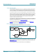
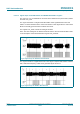
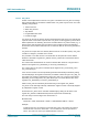
Table Of Contents
- 1. General description
- 2. Features and benefits
- 3. Applications
- 4. Quick reference data
- 5. Ordering information
- 6. Block diagram
- 7. Pinning information
- 8. Functional description
- 8.1 80C51
- 8.2 General purpose IOs configurations
- 8.3 Host interfaces
- 8.4 Power management
- 8.5 Power clock and reset controller
- 8.6 Contactless Interface Unit (CIU)
- 8.6.1 Feature list
- 8.6.2 Simplified block diagram
- 8.6.3 Reader/Writer modes
- 8.6.4 ISO/IEC 18092, ECMA 340 NFCIP-1 operating mode
- 8.6.5 Card operating modes
- 8.6.6 Overall CIU block diagram
- 8.6.7 Transmitter control
- 8.6.8 RF level detector
- 8.6.9 Antenna presence self test
- 8.6.10 Random generator
- 8.6.11 Data mode detector
- 8.6.12 Serial data switch
- 8.6.13 NFC-WI/S2C interface support
- 8.6.14 Hardware support for FeliCa and NFC polling
- 8.6.15 CRC co-processor
- 8.6.16 FIFO buffer
- 8.6.17 CIU_timer
- 8.6.18 Interrupt request system
- 8.6.19 CIU Power Reduction Modes
- 8.6.20 CIU command set
- 8.6.20.1 General description
- 8.6.20.2 General behavior
- 8.6.20.3 Commands overview
- 8.6.20.4 Idle command
- 8.6.20.5 Config command
- 8.6.20.6 Generate RandomID command
- 8.6.20.7 CalcCRC command
- 8.6.20.8 Transmit command
- 8.6.20.9 NoCmdChange command
- 8.6.20.10 Receive command
- 8.6.20.11 Transceive command
- 8.6.20.12 AutoColl command
- 8.6.20.13 MFAuthent command
- 8.6.20.14 SoftReset command
- 8.6.21 CIU tests signals
- 8.6.22 CIU memory map
- 8.6.23 CIU register description
- 8.6.23.1 CIU register bit behavior
- 8.6.23.2 CIU_SIC_CLK_en register (6330h)
- 8.6.23.3 CIU_Command register (D1h or 6331h)
- 8.6.23.4 CIU_CommIEn register (D2h or 6332h)
- 8.6.23.5 CIU_DivIEn register (D3h or 6333h)
- 8.6.23.6 CIU_CommIrq register (D4h or 6334h)
- 8.6.23.7 CIU_DivIrq register (D5h or 6335h)
- 8.6.23.8 CIU_Error register (D6h or 6336h)
- 8.6.23.9 CIU_Status1 register (DFh or 6337h)
- 8.6.23.10 CIU_Status2 register (E9h or 6338h)
- 8.6.23.11 CIU_FIFOData register (EAh or 6339h)
- 8.6.23.12 CIU_FIFOLevel register (EBh or 633Ah)
- 8.6.23.13 CIU_WaterLevel register (ECh or 633Bh)
- 8.6.23.14 CIU_Control register (EDh or 633Ch)
- 8.6.23.15 CIU_BitFraming register (EEh or 633Dh)
- 8.6.23.16 CIU_Coll register (EFh or 633Eh)
- 8.6.23.17 CIU_Mode register (6301h)
- 8.6.23.18 CIU_TxMode register (6302h)
- 8.6.23.19 CIU_RxMode register (6303h)
- 8.6.23.20 CIU_TxControl register (6304h)
- 8.6.23.21 CIU_TxAuto register (6305h)
- 8.6.23.22 CIU_TxSel register (6306h)
- 8.6.23.23 CIU_RxSel register (6307h)
- 8.6.23.24 CIU_RxThreshold register (6308h)
- 8.6.23.25 CIU_Demod register (6309h)
- 8.6.23.26 CIU_FelNFC1 register (630Ah)
- 8.6.23.27 CIU_FelNFC2 register (630Bh)
- 8.6.23.28 CIU_MifNFC register (630Ch)
- 8.6.23.29 CIU_ManualRCV register (630Dh)
- 8.6.23.30 CIU_TypeB register (630Eh)
- 8.6.23.31 CIU_CRCResultMSB register (6311h)
- 8.6.23.32 CIU_CRCResultLSB register (6312h)
- 8.6.23.33 CIU_GsNOff register (6313h)
- 8.6.23.34 CIU_ModWidth register (6314h)
- 8.6.23.35 CIU_TxBitPhase register (6315h)
- 8.6.23.36 CIU_RFCfg register (6316h)
- 8.6.23.37 CIU_GsNOn register (6317h)
- 8.6.23.38 CIU_CWGsP register (6318h)
- 8.6.23.39 CIU_ModGsP register (6319h)
- 8.6.23.40 CIU_TMode register (631Ah)
- 8.6.23.41 CIU_TPrescaler register (631Bh)
- 8.6.23.42 CIU_TReload_hi register (631Ch)
- 8.6.23.43 CIU_TReloadVal_lo register (631Dh)
- 8.6.23.44 CIU_TCounterVal_hi register (631Eh)
- 8.6.23.45 Register CIU_TCounterVal_lo (631Fh)
- 8.6.23.46 CIU_TestSel1 register (6321h)
- 8.6.23.47 CIU_TestSel2 register (6322h)
- 8.6.23.48 CIU_TestPinEn register (6323h)
- 8.6.23.49 CIU_TestPinValue register (6324h)
- 8.6.23.50 CIU_TestBus register (6325h)
- 8.6.23.51 CIU_AutoTest register (6326h)
- 8.6.23.52 CIU_Version register (6327h)
- 8.6.23.53 CIU_AnalogTest register (6328h)
- 8.6.23.54 CIU_TestDAC1 register (6329h)
- 8.6.23.55 CIU_TestDAC2 register (632Ah)
- 8.6.23.56 CIU_TestADC register (632Bh)
- 8.6.23.57 CIU_RFlevelDet register (632Fh)
- 8.7 Registers map
- 9. Limiting values
- 10. Recommended operating conditions
- 11. Thermal characteristics
- 12. Characteristics
- 12.1 Power management characteristics
- 12.2 Overcurrent detection
- 12.3 Current consumption characteristics
- 12.4 Antenna presence self test thresholds
- 12.5 Typical 27.12 MHz Crystal requirements
- 12.6 Pin characteristics for 27.12 MHz XTAL Oscillator (OSCIN, OSCOUT)
- 12.7 RSTPD_N input pin characteristics
- 12.8 Input pin characteristics for I0 and I1
- 12.9 RSTOUT_N output pin characteristics
- 12.10 Input/output characteristics for pin P70_IRQ
- 12.11 Input/output pin characteristics for P30 / UART_RX, P31 / UART_TX, P32_INT0, P33_INT1
- 12.12 Input/output pin characteristics for P34 / SIC_CLK
- 12.13 Input/output pin characteristics for P35
- 12.14 Input pin characteristics for NSS / P50_SCL / HSU_RX
- 12.15 Input/output pin characteristics for MOSI / SDA / HSU_TX
- 12.16 Input/output pin characteristics for MISO / P71 and SCK / P72
- 12.17 Input pin characteristics for SIGIN
- 12.18 Output pin characteristics for SIGOUT
- 12.19 Output pin characteristics for LOADMOD
- 12.20 Input pin characteristics for RX
- 12.21 Output pin characteristics for AUX1/AUX2
- 12.22 Output pin characteristics for TX1/TX2
- 12.23 Timing for Reset and Hard-Power-Down
- 12.24 Timing for the SPI compatible interface
- 12.25 Timing for the I2C interface
- 13. Application information
- 14. Package outline
- 15. Abbreviations
- 16. Revision history
- 17. Legal information
- 18. Contact information
- 19. Contents

PN532_C1 All information provided in this document is subject to legal disclaimers. © NXP B.V. 2017. All rights reserved.
Product data sheet
COMPANY PUBLIC
Rev. 3.6 — 28 November 2017
115436 123 of 222
NXP Semiconductors
PN532/C1
Near Field Communication (NFC) controller
8.6.13 NFC-WI/S
2
C interface support
The NFC-WI/S
2
C provides the possibility to directly connect a secure IC to the PN532 in
order to act as a contactless smart card IC via the PN532. The interfacing signals can be
routed to the pins SIGIN and SIGOUT. SIGIN can receive either a digital FeliCa or digital
ISO/IEC 14443A signal sent by the secure IC. The SIGOUT pin can provide a digital
signal and a clock to communicate to the secure IC. A secure IC can be a smart card IC
provided by NXP Semiconductors.
The PN532 generates the supply SVDD to the secure IC. The pins SIGIN and SIGOUT
are referred to this supply, as well as pin P34 / SIC_CLK, which can be used as an extra
pin for the connection to a secure IC.
The following figure outlines the supported communication flows via the PN532 to the
secure core IC.
Configured in the Wired Card mode the host controller can directly communicate to the
secure IC via SIGIN/SIGOUT. In this mode the PN532 generates the RF clock and
performs the communication on the SIGOUT line. To enable the Wired Card mode the
clock has to be derived by the internal oscillator of the PN532 (see bits sic_clock_sel in
Table 265 on page 181
.)
Configured in Card emulation mode the secure IC can act as contactless smart card IC
via the PN532. In this mode the signal on the SIGOUT line is provided by the RF field of
the external Reader/Writer. To enable the Virtual Card mode the clock derived by the
external RF field has to be used.
The configuration of the NFC-WI/S
2
C interface differs for the FeliCa and MIFARE scheme
as outlined in the following chapters.
Fig 41. Communication flows supported by the NFC-WI interface
80C51
Host
Host Interfaces
FIFO and state machine
Serial Data Switch
secure IC
P34
SIGOUT
SIGIN
1. Wired Card mode
2. Card emulation mode
PN532
Analog + CL UART
CIU
(Virtual Card mode)