
Datasheet
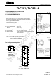


TLP281,TLP281-4
3 2019-06-17
© 2019
Toshiba Electronic Devices & Storage Corporation
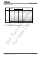
Absolute Maximum Ratings
(Ta = 25°C)
CHARACTERISTIC SYMBOL
RATING
UNIT
TLP281
TLP281-4
LED
Forward Current I
F
50 mA
Forward Current Derating ∆I
F
/°C -0.7 (Ta≥53°C) -0.5 (Ta≥25°C) mA/°C
Pulse Forward Current
(100 μs pulse, 100 pps)
I
FP
1 A
Reverse Voltage V
R
5 V
Diode power dissipation
P
D
100 70 mW
Diode power dissipation derating
∆
P
D
/°C -1.39 (Ta≥53°C) -0.7
(Ta≥25°C) mW/°C
Junction Temperature T
j
125 °C
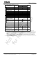
DETECTOR
Collector-Emitter Voltage V
CEO
80 V
Emitter-Collector Voltage V
ECO
7 V
Collector Current I
C
50 mA
Collector Power Dissipation
(1 Circuit)
P
C
150 100 mW
Collector Power Dissipation
Derating(Ta≥25°C) (1 Circuit)
∆P
C
/°C -1.5 -1.0 mW/°C
Junction Temperature T
j
125 °C
Operating Temperature Range T
opr
-55 to 100 °C
Storage Temperature Range T
stg
-55 to 125 °C
Lead Soldering Temperature (10 s) T
sol
260 °C
Total Package Power Dissipation
(1 Circuit)
P
T
200 170 mW
Total Package Power Dissipation
Derating (Ta≥25°C) (1 Circuit)
∆P
T
/°C -2.0 -1.7 mW/°C
Isolation Voltage
(AC, 60 s, R.H.≤ 60 %) (Note 1)
BV
S
2500
Vrms
Note: Using continuously under heavy loads (e.g. the application of high temperature/current/voltage and the
significant change in temperature, etc.) may cause this product to decrease in the reliability significantly even
if the operating conditions (i.e. operating temperature/current/voltage, etc.) are within the absolute maximum
ratings.
Please design the appropriate reliability upon reviewing the Toshiba Semiconductor Reliability Handbook
(“Handling Precautions”/“Derating Concept and Methods”) and individual reliability data (i.e. reliability test
report and estimated failure rate, etc).
Note 1: Device considered a two terminal device : LED side pins shorted together and DETECTOR side pins shorted
together.