
User Guide

MPLAB
®
PICkit™ 4 User’s Guide
DS50002751C-page 20 2018 Microchip Technology Inc.
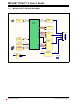
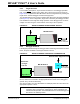
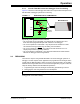
A simplified diagram of some of the internal interface circuitry of the MPLAB PICkit 4
In-Circuit Debugger is shown.
FIGURE 2-8: PROPER CONNECTIONS FOR PROGRAMMING
For programming, no clock is needed on the target device, but power must be supplied.
When programming, the debugger puts programming levels on V
PP/MCLR, sends
clock pulses on PGC and serial data via PGD. To verify that the part has been
programmed correctly, clocks are sent to PGC and data is read back from PGD. This
sequence confirms the debugger and device are communicating correctly.
2.5 REQUIREMENTS FOR DEBUGGING
To debug (set breakpoints, see registers, etc.) with the MPLAB PICkit 4 In-Circuit
Debugger system, there are critical elements that must be working correctly:
• The debugger must be connected to a computer. It must be powered by the
computer via the USB cable and it must be communicating with the MPLAB X IDE
software via the Micro-B USB cable. See Section 3.3 “Debug Tutorial” for
details.
• The debugger must be connected as shown in Figure 2-8 to the Vpp, PGC and
PGD pins of the target device with the modular interface cable (or equivalent).
• The target device must have power and a functional, running oscillator. If the
target device does not run, for any reason, the MPLAB PICkit 4 In-Circuit
Debugger cannot debug.
• The target device must have its configuration words programmed correctly. These
are set using the MPLAB X IDE.
- The oscillator Configuration bits should correspond to RC, XT, etc., depending
upon the target design.
- For some devices, the Watchdog Timer is enabled by default and needs to be
disabled.
- The target device must not have code protection enabled.
- The target device must not have table read protection enabled.
- For some devices with more than one PGC/PGD pair, the correct pair needs
to be selected in the device’s configuration word settings. This only refers to
debugging, since programming will work through any PGC/PGD pair.
When the conditions listed above are met, you may proceed to the following:
• Sequence of Operations Leading to Debugging
• Debugging Details
+5V
Programming
VPP/MCLR
PGC
PGD
1
5
4
Internal Circuits
VSS
VDD
Voltage