
Data Sheet


CP2102
6 Rev. 1.1
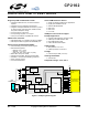
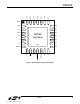
4. Pinout and Package Definitions
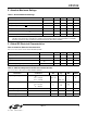
Table 4. CP2102 Pin Definitions
Name Pin # Type Description
V
DD
6 Power In
Power Out
3.0–3.6 V Power Supply Voltage Input.
3.3 V Voltage Regulator Output. See <PDF link>Section 10.
GND 3 Ground
RST 9 D I/O Device Reset. Open-drain output of internal POR or V
DD
monitor.
An external source can initiate a system reset by driving this pin low
for at least 15 µs.
REGIN 7 Power In 5 V Regulator Input. This pin is the input to the on-chip voltage reg-
ulator.
VBUS 8 D In VBUS Sense Input. This pin should be connected to the VBUS sig-
nal of a USB network. A 5 V signal on this pin indicates a USB net-
work connection.
D+ 4 D I/O USB D+
D– 5 D I/O USB D–
TXD 26 D Out Asynchronous data output (UART Transmit)
RXD 25 D In Asynchronous data input (UART Receive)
CTS 23* D In Clear To Send control input (active low)
RTS 24* D Out Ready to Send control output (active low)
DSR 27* D in Data Set Ready control input (active low)
DTR 28* D Out Data Terminal Ready control output (active low)
DCD 1* D In Data Carrier Detect control input (active low)
RI 2* D In Ring Indicator control input (active low)
SUSPEND 12* D Out This pin is driven high when the CP2102 enters the USB suspend
state.
SUSPEND
11* D Out This pin is driven low when the CP2102 enters the USB suspend
state.
NC 10, 13–22 These pins should be left unconnected or tied to V
DD
.
*Note: Pins can be left unconnected when not used.