
Specifications


5.4. HARDWARE
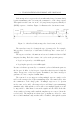
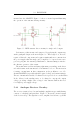
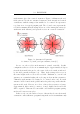
Figure 5.6: RFID antenna driver circuitry using push-pull output stage
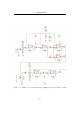
resonant circuit, tuned to 130kHz. Thereafter, the signal is again amplified
into saturation to provide a 5V logic level square-wave representation of the
received signal. B ased on the width of the pulses, the frequency of the signal
can be determined (see Section 5.5 for details of this calculation).
Recall that the potential across the antenna terminals is likely to be in the
order of hundreds of volts due to the high-Q nature of the tuned circuit. It is
thus impossible to feed this voltage directly into any low voltage component
such as an opamp. The solution is to AC couple the antenna through a
resistor and then diode-clamp the signal at supply levels before feeding it
into the first amplifier stage. Due to the relatively high input impedance
(1kΩ), the operation of the receiver does not significantly impact the tuning
of the transmitter output stage, and the same antenna can thus be used for
sending and receiving. This does, however, mean that the antenna must be
capable of receiving both the 123.4kHz and 134.2kHz signals. The “Q” of the
circuit is thus limited by the required bandwidth of approximately 10kHz.
The LF353 dual FET input op-amp was chosen as the primary amplifier
mainly due to its high bandwidth product and high input impedances coupled
with its low cost. Two of these devices form the first amplifier stages, before
the tuned filter. The total gain of this stage is 1000. Both LF353 s are
powered directly from the 12V battery rather than the 5V logic rail to provide
additional headroom for the signal. Although this supply is unregulated, the
battery represents a low-impedance source and during the receive phase, the
high-current transmitters are disabled. Thus, the 12V remains smooth (as
opposed to the 5V rail which powers digital logic from a SMPS). The non-
inverting inputs of these op-amps are biased at half of the supply and each
34