
Specifications


5.4. HARDWARE
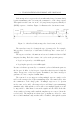
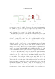
in turn drive the MOSFET. Figure 5.5 shows a circuit diagram illustrating
the operation of the antenna driving circuitry:
Figure 5.5: RFID antenna driver circuitry for single ended output
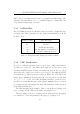
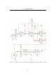
Performance of this circuit can be improved by replacing the output stage
with a push-pull design as shown in Figure 5.6. This design does, however,
require additional components and requires significantly more current from
the power supply than the single ended output (to be expected since more
power is going into the antenna!). Furthermore, antenna tuning is critical to
the efficient operation of the circuit.
The transformer is self-wound using eight turns per winding on the driver
side and 16 turns on the antenna side on an 18mm toroid core. The motivation
for using a transformer in this configuration is the prohibitive cost of P-
channel MOSFETs (especially with the required voltage and current ratings).
The use of transformers and two N-channel devices provide a low cost alternative.
It also allows for the winding ratios to be changed to step-up the output
voltage, providing a higher drive voltage for the antenna without the need
for a higher power supply voltage.
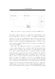
5.4.3 Analogue Receiver Circuitry
The receiver circuit is based around multiple amplifier stages with filtering
courtesy of a high-Q bandpass filter. Figure 5.7 shows the circuit diagram
of the receiver stage. The signal is received, amplified and fed into a parallel
33