
Specifications

Appendix A
Appendix: RFID Receiver
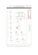
A.1 PCB Layout of Push-pull Output Reader
with Single-channel Receiver
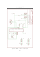
Figure A.1 shows a reduced circuit diagram for a push-pull output reader with
one receiver channel. A full-size schematic can be found on the attached CD.
Figure A.2 shows the PCB layout. The design of this reader is discussed in
Section 5.4.
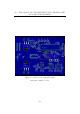
A.2 PCB Layout of Single-ended Output Reader
with Dual-channel Rece iver
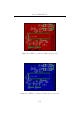
Figure A.3 shows the PCB circuit layout of a dual-channel receiver with
single-ended outputs. The circuit diagram can be found on the attached CD.
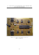
Figure A.4 shows a populated board, without a top silkscreen or tuned filters.
The details of this design can be found in Section 5.4.
A-1