
Specifications
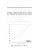

8.3. REGULATOR SELECTION
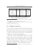
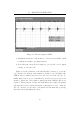
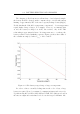
Figure 8.1: DC rail output of SMPS.
• Adjustment in the size of the inductor - decrease from 260µH to 80µH
to suit the new higher operating frequency.
• Feedback resistor network was adjusted to provide the correct output
voltages of 3.8V and 5.0V.
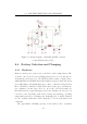
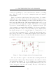
Figure 8.2 is the schematic of the final DC-DC converter to power the
logic circuits. Note that two such circuits are required: one 3.8V unit for the
GSM module as outlined in Section 7.3.1 and a second for the 5V logic. To
further improve the device’s overall efficiency, it was decided to provide a soft
switch to disable the 3.8V regulator entirely when the GSM module is not
required. This is prudent, because the GSM unit is not required frequently
and the L4976 draws a quiescent current of 4mA under no-load conditions.
The 5V converter does not have a soft-switch and automatically p owers-up
when the battery has sufficient voltage.
93