
Datasheet


WPMDB1200362Q / 171020302
MagI
3
C Power Module
VDRM – Variable Step Down Regulator Module
we-online.com Würth Elektronik eiSos GmbH & Co. KG – Data Sheet Rev. 1.0
© May 2016 25/48
In order to choose the value of the output capacitor, the following steps should be utilized:
1. According to the operating conditions (V
IN
, V
OUT
and f
SW
), select the minimum C
OUT
recommended in table on
page 35.
2. Measure t
d
.
3. Calculate the appropriate value of C
OUT
for the maximum voltage drop V
discharge
allowed at a defined load step,
using the following equation (10), derived from equation (9):
C
≥
∆I
∙t
2∙V
(10)
4. As above mentioned, changing C
OUT
affects also t
d
. Therefore a new measurement should be performed and, if
necessary, the step 2 and 3 should be repeated (it is an iterative process and few steps could be required).
Example. V
IN
= 5V, V
OUT
= 3.3V, ΔI
OUT
= 1A, f
sw
= 1.5MHz, ΔV
OUT
<0.1V.
According to the table on page 35, an output MLCC of 47µF would be necessary. After mounting this capacitor, the load
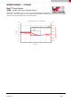
transient should be performed and the t
d
measured (see picture below).
The ΔV
OUT
= 0.12V and t
d
= 7µs. It is important to remind that the ΔV
OUT
includes also the voltage drop during t
rise
, mainly due
to the ESR (V
ESR
= 20mV, see picture above). In order to achieve the desired maximum ΔV
OUT
, the V
discharge
should be below
0.06V. Using the equation (9), the minimum required output capacitor is:
C
≥
1A ∙7μs
2∙0.06V
=58μF
To achieve the calculated value of C
OUT
an additional MLCC of 47µF is mounted in parallel (considering the lower effective
capacitance due to DC biasing).
-0,30
-0,20
-0,10
0,00
0,10
0,20
0,30
-2,0
-1,5
-1,0
-0,5
0,0
0,5
1,0
1,5
2,0
0 10 20 30 40 50 60
V
OUT
(AC coupled) [V]
I
OUT
[A]
time [µs]
Load transient with C
OUT
= 47µF MLCC
ΔV
OUT
= 0.12V
7µs
V
discharge
= 0.1V
V
OUT
I
OUT