
User Manual
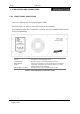
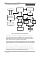
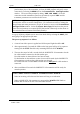
Table Of Contents

Vytek PTX-150
Doc Ref : 7M393-1 Version C1 Page : 4
VYTEK - 2000
1.3 DESCRIPTION OF OPERATION
INTRODUCTION
Figure 1.3.1 Block Diagram of the Paging Transmitter
A block diagram of the operation of the paging transmitter is shown in figure 1.3.1.
On the exciter printed circuit board, the DDS/DSP circuitry generates a 10.7 MHz
modulated signal, referenced to the internal TCXO or an external reference frequency
source. (The reference source is selected in a software option).
The external reference is only required when stability of the carrier better than ±1PPM is
required. (Parameters such as rise time, absolute deviation, mode etc are all selectable in
software).
The 10.7 MHz modulated signal is processed through a filter before being applied to the
first mixer. The LO input to the first mixer is a high quality 235 MHz un-modulated
signal with very low phase noise. The mixing products are filtered and buffered with two
stages of SAW filtering, and the low side product of 224.3 MHz is then applied to the
second mixer. The Second mixer LO frequency is equal to final frequency + 224.3 MHz.
Channel change is effected by the VCO supplying the second mixer.
External Freq. standard.
(optional)
DSP/DDS circuits,
microprocessor,
modulator and TCXO
Frequency converter
and mixer
VCO and channel
synthesizer
RF filter and
preamp.Nominal 300
mW/50 ohms
20 Watt Driver
Amplifier.
AC Power supply
(optional)
37 pin DIN
Auto Diagnostics
Circuits
Power Splitter
75 Watt
Power
Amplifier
75 Watt
Power
Amplifier
Combiner
Filter
RF OUT