
User Manual

Power Amplifier Serial I/F Spec.
12 Version 1.62
During the 5 byte transfer, A5-A0 will not normally change.
If prior to the completion of the 5 byte transfer, the SPI address A5..A0 changes, for example
due to a host reset or error, the transfer will be halted by the PA. The next time the device ID on
the addressed PA is active, the transfer begins again starting with byte 1.
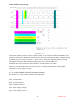
The timing diagram is shown in Figure 3-3:
0Figure 3-3
3.7.2 Power Amplifier DeviceID 1 transfer protocol
DeviceID 1 is a 1 byte transfer. The timing diagram for this transfer is shown in Figure 3-2.
3.7.3 Power Amplifier DeviceID 2 transfer protocol
DeviceID 2 is a 1 byte transfer. The timing diagram for this transfer is shown in Figure 3-2.
3.7.4 Power Amplifier DeviceID 3 transfer protocol
DeviceID 3 is a 1 byte transfer. The timing diagram for this transfer is shown in Figure 3-2.
3.7.5 Power Amplifier DeviceID 4 transfer protocol
3.7.5.1 Read
A read of DeviceID 4 is a 6 byte transfer with the following order:
Byte 1: 0x03 (this is the READ instruction byte for the EEPROM)
Byte 2: target EEPROM page number (0-63) shifted left two bits (e.g page 3 = 00001100b)
Byte 3: byte 1
Byte 4: byte 2