
User Manual

Power Amplifier Serial I/F Spec.
13 Version 1.62
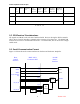
Byte 5: byte 3
Byte 6: byte 4
The timing diagram for this transfer is approximately shown in Figure 3-3, with the addition of a
byte.
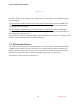
3.7.5.2 Write
A write to DeviceID 4 is an 8 byte transfer with the following order:
Byte 1: 0x06 (this is the WRITE ENABLE instruction byte for the EEPROM)
Byte 2: 0x02 (this is the WRITE instruction byte for the EEPROM)
Byte 3: target EEPROM page number (0-63) shifted left two bits (e.g page 63 = 11111100b)
Byte 4: byte 1
Byte 5: byte 2
Byte 6: byte 3
Byte 7: byte 4
Byte 8: 0x04 (this is the WRITE DISABLE instruction byte for the EEPROM)
The timing diagram for this transfer is approximately shown in Figure 3-3, with the addition of 3
bytes.