SM7100 MICROWAVE MATRIX USER’S MANUAL P/N: 82-0055-000 Released February 13, 2006 VXI Technology, Inc.
VXI Technology, Inc.
www.vxitech.com TABLE OF CONTENTS INDTRODUCTION TABLE OF CONTENTS ................................................................................................................................................3 Certification ..........................................................................................................................................................4 Warranty ........................................................................................................................
VXI Technology, Inc. CERTIFICATION VXI Technology, Inc. (VTI) certifies that this product met its published specifications at the time of shipment from the factory. VTI further certifies that its calibration measurements are traceable to the United States National Institute of Standards and Technology (formerly National Bureau of Standards), to the extent allowed by that organization’s calibration facility, and to the calibration facilities of other International Standards Organization members.
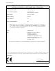
www.vxitech.com DECLARATION OF CONFORMITY Declaration of Conformity According to ISO/IEC Guide 22 and EN 45014 MANUFACTURER’S NAME VXI Technology, Inc. MANUFACTURER’S ADDRESS 2031 Main Street Irvine, California 92614-6509 PRODUCT NAME Microwave Matrix MODEL NUMBER(S) SM7100 PRODUCT OPTIONS All PRODUCT CONFIGURATIONS All VXI Technology, Inc.
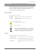
VXI Technology, Inc. GENERAL SAFETY INSTRUCTIONS Review the following safety precautions to avoid bodily injury and/or damage to the product. These precautions must be observed during all phases of operation or service of this product. Failure to comply with these precautions, or with specific warnings elsewhere in this manual, violates safety standards of design, manufacture, and intended use of the product. Service should only be performed by qualified personnel.
www.vxitech.com WARNINGS (CONT.) Avoid Electric Shock To avoid electric shock or fire hazard, do not operate this product with the covers removed. Do not connect or disconnect any cable, probes, test leads, etc. while they are connected to a voltage source. Remove all power and unplug unit before performing any service. Service should only be performed by qualified personnel. Ground the Product This product is grounded through the grounding conductor of the power cord.
VXI Technology, Inc. SUPPORT RESOURCES Support resources for this product are available on the Internet and at VXI Technology customer support centers. VXI Technology World Headquarters VXI Technology, Inc. 2031 Main Street Irvine, CA 92614-6509 Phone: (949) 955-1894 Fax: (949) 955-3041 VXI Technology Cleveland Instrument Division 5425 Warner Road Suite 13 Valley View, OH 44125 Phone: (216) 447-8950 Fax: (216) 447-8951 VXI Technology Lake Stevens Instrument Division VXI Technology, Inc.
www.vxitech.com SECTION 1 INTRODUCTION OVERVIEW The SM7100 Microwave Matrix is a member of the VXI Technology SMIP II™ (Switch Modularity Interface Platform) family. It offers a modular design allowing custom switching configurations in a single chassis. The SM7100 is a double-wide, C-size VXI module, which can support customized microwave switch configurations for many applications.
VXI Technology, Inc. Programmable Timing Delays A delay can be programmed between relay closures to allow for settling times of other system resources. When used with triggers, a controlled synchronous switching system can easily be configured. Safety Interrupt This is a programmable fail-safe feature that allows all relays to open based upon the occurrence of a selected TTL backplane trigger.
www.vxitech.com SECTION 2 PREPARATION FOR USE INTRODUCTION When the SMIP is unpacked from its shipping carton, the contents should include the following items: (1) SMIP VXIbus module (1) SM7100 Microwave Matrix User’s Manual (this manual) All components should be immediately inspected for damage upon receipt of the unit. Once the SMIP II is assessed to be in good condition, it may be installed into an appropriate Csize or D-size VXIbus chassis in any slot other than slot zero.
VXI Technology, Inc. SETTING THE LOGICAL ADDRESS The logical address of the SMIP II is set by two rotary switches located on the top edge of the interface card, near the backplane connectors. Each switch is labeled with positions 0 through F. The switch closer to the front panel of the module is the least significant bit (LSB or “Front”), and the switch located towards the back of the module is the most significant bit (MSB or “Back”).
www.vxitech.com Example 2 200 / 16 LSB = 12 w/ 8 remaining Divide by 16. = 1100 1000 Convert to MSB and LSB. = C 8 Convert to hexadecimal. Set the back switch to C and the front switch to 8.
VXI Technology, Inc.
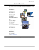
www.vxitech.com SECTION 3 SWITCH CONFIGURATION FRONT PANEL CONNECTION - SM7000 PWR/ FAIL ACC/ ERR SM7100 EXPANDABLE MICROWAVE SWITCH MATRIX This section details the SM7100 schematics, relays, and pinouts. See Section 4, Programming, for information on relay addressing. NOTE INPUTS 2 1 Although pin numbers between the SM7000 and the HP equivalent differ, the signals remain in the same location. This makes it possible to use the same mating connector and cabling for either system.
VXI Technology, Inc.
www.vxitech.
VXI Technology, Inc.
www.vxitech.
VXI Technology, Inc.
www.vxitech.com SECTION 4 PROGRAMMING REGISTER ACCESS The SMIP II modules are VXIbus register-based devices for high-speed data transfers. Registerbased programming is a series of reads and writes directly to the switch module registers. This eliminates the time for command parsing thus increasing speed. ADDRESSING The VTI switching modules utilize either the A24 or A32 space of the shared-memory architecture. To read or write to a module register, a register address needs to be specified.
VXI Technology, Inc.
www.vxitech.com DESCRIPTION OF REGISTERS - A16 The following describes the registers shown in the SMIP II Register Map for A16 address space. ID Register (0x00) — Read Only D11-D0 Manufacturer's ID D13-D12 Address Space D15-D14 Device Class VXI Technology, Inc., set to F4B16 A16/A24 = 002 A16/A32 = 012 Extended register based device, set to 012 Logical Address Register (0x00) — Write Only D7-D0 Logical Address D15-D8 Reserved Sets the new logical address in a dynamically configured module.
VXI Technology, Inc. Offset Register (0x06) — Read and Write D15-D0 The value written to this 16-bit register, times 256, sets the base address of the A24 memory space used by the module. The value written to this 16-bit register, times 65,536, sets the base address of the A32 memory space used by the module. A read from this register reflects the previously written value. Because of the required memory size, bits D4 - D0 are disregarded on writes and always read back as 0.
www.vxitech.com Interrupt Control Register (0x1C) — Read and Write 0 = enabled 1 = disabled 0 = enabled D14 1 = disabled D13-D9 Data written to these bits has no effect 0 = enabled D8 Module Busy Complete 1 = disabled 0 = writing a 0 to this bit enables interrupter capabilities D7 IR ENA* 1 = writing a 1 to this bit disables interrupter capabilities The module has no interrupt handler capability; therefore writing a 1 or D6 IH ENA* 0 has no effect. A 1 is always read back for this bit.
VXI Technology, Inc. Trace RAM Start High Register (0x28) — Read and Write D15-D4 Unused D3-D0 Data written to these bits have no effect and always read back as 1. Sets the four most significant bits of the starting address of the Trace RAM, allowing the available RAM to be divided into multiple traces. Trace RAM Start Low Register (0x2A) — Read and Write Sets the 16 least significant bits of the starting address of the Trace RAM, allowing the available RAM to be divided into multiple traces.
www.vxitech.com Open Trigger Select Register (0x36) —Write Only Sets the TTLTRIG line or lines, which are configures as outputs, and will toggle when Relay Open condition occurs in the module. D15 corresponds to TTLTRIG7, D14 to TTLTRIG6, … and D8 to TTLTRIG0. Setting a bit to a 1 enables the trigger line, setting a bit to 0 disables the corresponding line. All bits are set to 0 when either a soft or a hard reset is received by the module.
VXI Technology, Inc. Busy Trigger Control Register (0x3C) — Read and Write D15-D8 TTLTRIG Select D7-D1 Unused D0 Busy Trigger Enable Sets the TTLTRIG Line or Lines, which are configured as outputs, and will toggle at the de-assertion of a Board Busy condition sent by the plug-in modules. D15 corresponds to TTLTRIG7, D14 to TTLTRIG6, … and D8 to TTLTRIG0. Setting a bit to a 1 enables the trigger line, setting a bit to a 0 disables the corresponding line.
www.vxitech.com DESCRIPTION OF SMIP II MODULE REGISTERS - A24 / A32 - EXTENDED MEMORY Each module is assigned 1 k (1024) bytes of memory as shown in the SMIP II Configuration/Relay Register Map for A24/A32 address space. The upper 512 bytes of memory space is used for module configuration registers. The following describes these registers.
VXI Technology, Inc. Control Register - Read and Write (continued) 0 = BBM (Break-Before-Make) / MBB (Make-Before-Break) is disabled 1 = BBM/MBB operation is enabled Pon state = 0 NOTE: This bit should remain a 0 (disabled) for the SM7100. If this bit is set, the relays will be sequenced to effect proper BBM or MBB operation. If this bit is not set, the module will process the newly written relay data as immediate data, writing it directly to the relay driver ports.
www.vxitech.com Control Register - Read and Write (continued) 0 = Non-inverted Front Panel Open signal polarity 1 = Inverted Front Panel Open signal polarity Pon state = 0 D1 Front Panel Open Signal Polarity Bit Non-inverted: If set in pulse mode, the Front Panel Open signal will generate a reset pulse on a falling edge. If set in level mode, the Front Panel Open signal will generate a reset signal on a low input signal.
VXI Technology, Inc. Delay Register - Read and Write ADDR D15-D0 Plug-In LA+0x202 This register is used to set the time that the plug-in module will hold the Board Busy signal active. The Board Busy signal is set every time the plug-in receives a Write to a relevant Relay Register memory space. The Board Busy signal will be removed at the end of the time out that is set by the value contained in this register. For each count loaded into this register, the Board Busy signal will be held active for 1 µs.
www.vxitech.com DEVICE MEMORY MAP RELAY REGISTER OFFSET The Relay Register Offset is located within the A24/32 address space of the module.
VXI Technology, Inc. PROGRAMMING With the introduction of VISA, sending a command to a register-based device is as simple as sending a command to a message-based device. Whether the application is graphical or standard, sending commands to the register-based device is just as intuitive.
www.vxitech.com INDEX A I A16 address space.............................................................23 A16 Base Address.............................................................21 A16 Offset Register ..........................................................21 A16 Offset Register Address ............................................21 A24 address space.............................................................21 A24 Base Address.............................................................
VXI Technology, Inc. U utilizing A32 extended memory space..............................34 V VISA.................................................................................34 VXIbus .......................................................................11, 21 VXIbus Extended Device .................................................25 W WEEE .................................................................................