
User`s guide


SMPS AC/DC Reference Design User’s Guide
DS70320B-page 64 © 2008 Microchip Technology Inc.
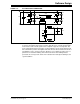
3.4.3 Secondary Side Software Time Management
The Single-Phase Buck Converter and Multi-Phase Buck Converter are both controlled
digitally by the same dsPIC DSC. Both converters operate at the same switching
frequency.
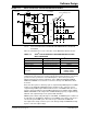
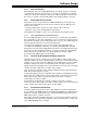
The two control loops are executed in an interleaved manner as shown in Figure 3-13.
The execution rate for each control loop is once every other PWM cycle. The execution
rate is determined by the execution times of each control loop.
The ADC ISR assumes the highest priority of all user software. Other interrupts are
assigned lower priority than the ADC interrupt, and all auxiliary software functions are
performed in the “Idle loop” (when the ADC interrupt is not being serviced).
FIGURE 3-13: INTERLEAVED CONTROL LOOP EXECUTION FOR SINGLE-PHASE AND
MULTI-PHASE BUCK CONVERTERS
3.5 AUXILIARY SOFTWARE ROUTINES
3.5.1 Output Sequencing
Many applications require specific turn-on and turn-off sequencing of power supplies
to ensure correct operation of the downstream electronics. The SMPS AC/DC
Reference Design implements power-on sequencing in the following order:
1. Initial start-up delay (allows all circuitry to stabilize after power-up).
2. PFC Converter ramps to around 420V.
3. Phase-Shift ZVT Converter ramps to 12V.
4. Single-Phase Buck Converter ramps to 5V.
5. Multi-Phase Buck Converter ramps to 3.3V.
PWM1H
PWM1L
PWM2H
PWM2L
PWM3H
PWM3L
PWM4H
PWM4L
3.3V Buck
Voltage Trigger
Execute
3.3V
Buck
Control
Loop
Sample
and
Convert
AN2, AN3
Idle
Loop
Execute
5V Buck
Control
Loop
Sample
and
Convert
AN0, AN1
Idle
Loop
5V Buck
Voltage Trigger
Execute
5V Buck
Control
Loop
Sample
and
Convert
AN0, AN1
Idle
Loop
5V Buck
Voltage Trigger
3.3V Buck
Voltage Trigger
Execute
3.3V
Buck
Control
Loop
Sample
and
Convert
AN2, AN3
Idle
Loop
Execute
5V Buck
Control
Loop
Idle
Loop
5V Buck
Voltage Trigger
3.3V Buck
Voltage Trigger
Execute
3.3V
Buck
Control
Loop
Sample
and
Convert
AN2, AN3
Sample
and
Convert
AN0, AN1