
User`s guide


Software Design
© 2008 Microchip Technology Inc. DS70320B-page 63
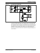
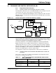
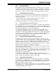
FIGURE 3-12: MULTI-PHASE BUCK CONVERTER PWM DRIVE SIGNALS
3.4.2.2 MULTI-PHASE BUCK CONVERTER IMPLEMENTATION USING THE
dsPIC DSC
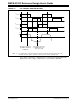
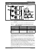
Table 3-5 summarizes the resource allocation for the Multi-Phase Buck Converter.
TABLE 3-5: dsPIC
®
DSC RESOURCE ALLOCATION FOR MULTI-PHASE
BUCK CONVERTER
The output voltage is measured from the analog input AN3. As this converter uses
voltage mode control, there is no need for current measurement. However, overcurrent
protection must be provided for each individual phase. Overcurrent protection is
implemented using the analog comparators on the dsPIC33FJ16GS504. CMP2A,
CMP3A and CMP4A are used for the overcurrent sensing for the Multi-Phase Buck
Converter.
Each of the three phases is driven by a pair of complementary PWM signals. The PWM
module on the dsPIC33FJ16GS504 provides a built-in mode to generate a pair of
complementary PWM outputs with dead time insertion. The PWM module also has a
feature to generate a Master Period and Master Duty Cycle for multiple outputs. PWM1,
PWM2, and PWM3 are all configured for a PWM switching frequency of approximately
500 kHz, and complementary mode operation with dead time.
PWM2 is phase advanced by 120 degrees from PWM1, and PWM3 is phase advanced
by 120 degrees from PWM2 (or 240 degrees from PWM1). The voltage control loop is
executed every two PWM cycles. The control loop is called from the ADC ISR.
The output of the voltage control loop is used to directly modify the PWM Master Duty
Cycle to control the output voltage.
12V Input
3.3V Output
GND
Q1
Q2
Q3
Q4
Q5
Q6
120º 120º 120º
Q1
Q3
Q5
Drive Signals are
Phase-Shifted by 120º
Description Type of Signal dsPIC
®
DSC Resource Used
Buck 1 Current Analog Comparator Input CMP2A
Buck 2 Current Analog Comparator Input CMP3A
Buck 3 Current Analog Comparator Input CMP4A
Buck Voltage Analog Input AN3
Multi-Phase Synchronous
Gate Drive
Drive Outputs PWM1H, PWM1L,
PWM2H, PWM2L,
PWM3H, PWM3L