
User`s guide


SMPS AC/DC Reference Design User’s Guide
DS70320B-page 62 © 2008 Microchip Technology Inc.
The output voltage is measured using the analog input AN1. The analog comparator
input CMP1A is connected to the output of the current transformer. The output voltage
is controlled by varying the duty cycle of PWM4.
The PWM4 pair is operated in Complementary mode with dead time. The switching
frequency is approximately 500 kHz. The duty cycle is controlled directly by the built-in
Cycle-by-Cycle Current-Limit mode and the analog comparator.
When the current-sense signal at the input of the analog comparator exceeds the
programmed comparator threshold, the PWM output is immediately terminated for the
remainder of the PWM cycle.
The Single-Phase Buck Converter circuitry is designed to operate in continuous
conduction mode at load currents greater than approximately 3A. If the Single-Phase
Buck Converter is operated in Discontinuous Conduction mode, the freewheeling
MOSFET is disabled through software.
At no load and light load current (< 3A), the PWM output may enter a “burst” mode. This
is caused by a low demand for load current by the converter in this range load current.
The voltage control loop is executed in the ADC ISR every two PWM cycles.
3.4.2 Multi-Phase Buck Converter
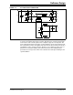
3.4.2.1 MULTI-PHASE BUCK CONVERTER CONTROL SCHEME
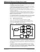
Voltage mode control is used for controlling the output of the Multi-Phase Buck
Converter on the SMPS AC/DC Reference Design. As shown in Figure 3-11, the
control scheme only implements a single control loop.
FIGURE 3-11: MULTI-PHASE BUCK CONVERTER CONTROL SCHEME
The output voltage is compared with the reference and results in a voltage error, which
is fed as an input to the voltage error compensator. The output of the voltage error
compensator modifies the duty cycle of all phases of the Multi-Phase Buck Converter.
The voltage error compensator is implemented as a PID function that is implemented
in the ADC ISR.
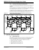
The Multi-Phase converter comprises of three individual phases, but the output is
controlled by a single duty cycle that identically drives the three phases. The PWM
drive signals for each phase are phase shifted by 120 degrees using the built-in PWM
phase-shifting feature available on the dsPIC33FJ16GS504. The PWM drive signals
for the Multi-Phase Buck Converter are shown in Figure 3-12.
Σ
+
-
Voltage
Reference
V
OUT
Phase 3
Inductor
Voltage Feedback
PWM
V
OUT
Sense
Voltage
Compensator
ADC
1001011011
S&H
Phase 2
Inductor
Phase 1
Inductor
Update
PWM
Cycle
PWM
PWM
Duty
Error