
User`s guide


Software Design
© 2008 Microchip Technology Inc. DS70320B-page 59
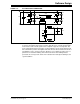
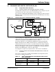
3.3.2.2 PHASE-SHIFT ZVT IMPLEMENTATION USING THE dsPIC DSC
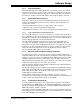
FIGURE 3-8: dsPIC
®
DSC RESOURCE ALLOCATION FOR PHASE-SHIFT ZVT CONVERTER
Table 3-2 lists the resources used on the primary side dsPIC DSC for the different
feedback and control signals required for the Phase-Shift ZVT Converter control
scheme. Table 3-3 lists resources used on the secondary side dsPIC DSC, also
required for the Phase-Shift ZVT Converter control scheme.
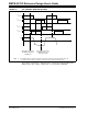
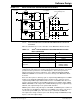
TABLE 3-2: PRIMARY SIDE dsPIC
®
DSC RESOURCES FOR PHASE-SHIFT
ZVT CONVERTER
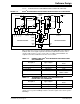
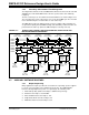
TABLE 3-3: SECONDARY SIDE dsPIC
®
DSC RESOURCES FOR
PHASE-SHIFT ZVT CONVERTER
The Phase-Shift ZVT Converter is controlled by modifying the phase of the PWM drive
signals of one leg of the Full-Bridge relative to the drive signals of the other leg of the
Full-Bridge.
k
1
k
2
ADC
Channel
ADC
Channel
UART
TX
PWM
UART
RX
PWM
PWM
IZVT
VHV_BUS
VOUT
Isolation
Barrier
ADC
Channel
PWM
PWM
PWM
FET
Driver
FET
Driver
FET
Driver
dsPIC33FJ16GS504
dsPIC33FJ16GS504
Description Type of Signal
dsPIC
®
DSC Resource
Used
ZVT Current 1 (I
ZVT1) Analog Input AN0
ZVT Current 2 (I
ZVT2) Analog Input AN2
V
OUT Feedback UART Input U1RX
Full-Bridge Gate Drive Drive Output PWM1H, PWM1L,
PWM2H, PWM2L
Synchronous Rectifier Gate Drive Drive Output PWM3H, PWM3L
Description Type of Signal
dsPIC
®
DSC Resource
Used
Voltage Sense (VOUT) Analog Input AN5
V
OUT Feedback UART Output U1TX