
User`s guide


SMPS AC/DC Reference Design User’s Guide
DS70320B-page 46 © 2008 Microchip Technology Inc.
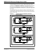
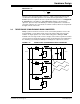
FIGURE 2-14: FLYBACK SMPS MOSFET WAVEFORMS
2.5.1 Basic Design Methodology
The target specification for the auxiliary flyback SMPS is as follows:
• Input voltage, V
IN = 120-400 VDC
• Primary Output Rail 1 = 7V @ 0.3A
• Primary Output Rail 2 = 13V @ 0.15A
• Secondary Output Rail 1 = 7V @ 0.3A
• Secondary Output Rail 2 = 17V @ 0.45A
2.5.1.1 HVIC TECHNOLOGY
The total output power rating of the auxiliary power supply is 13.8W; therefore, a Power
Integrations TinySwitch (see Reference 13 in Appendix C. “References”) was
selected for the main power switch. These devices are intended specifically for
low-cost high-efficiency designs and operate with simple ON/OFF control rather than
more sophisticated PWM common to higher power SMPS. The TNY277G is a suitably
rated part for this wide input voltage application, and can be mounted directly on the
PCB without any additional cooling requirements.
2.5.1.2 TRANSFORMER
Based on the operating frequency and power throughput requirement, an EF20 ferrite
core pair is selected for the transformer design. The first step in the design is to select
the number of primary turns and transformer air-gap. Discontinuous flyback SMPS
output power is dictated by the energy stored in the primary magnetizing inductance of
the transformer and the switching frequency. The basic equation, ignoring losses, is
shown in Equation 2-35.
EQUATION 2-35:
0 2.5 5 7.5 10 12.5 15
0
100
200
300
400
500
600
700
MOSFET Voltage (V)
Time ( s)
0 2.5 5 7.5 10 12.5 15
0
0.1
0.2
0.3
0.4
0.5
0.6
0.7
MOSFET Current (A)
Time ( s)
2
1
2
oppsw
P
LI f
=